


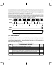
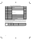
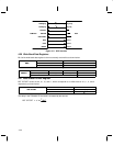

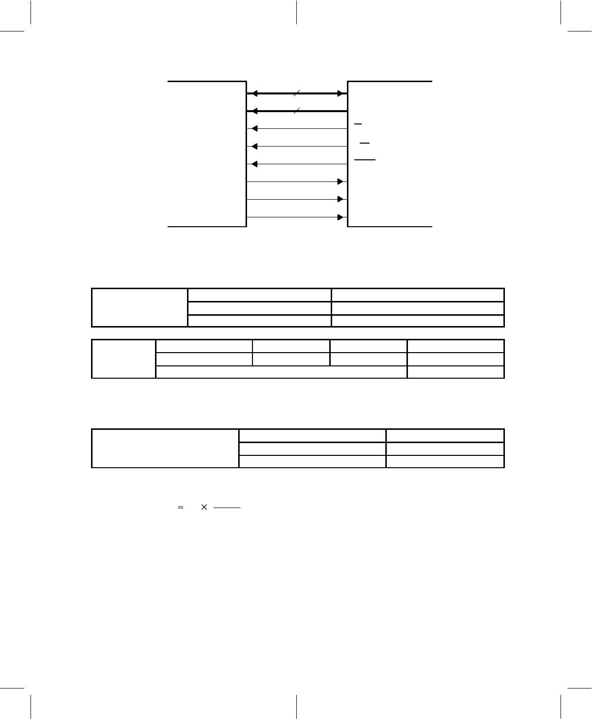
4–26
D[15:6]
A[3:0]
IS
R/W
STRB
INT 1
INT 3
INT 4
DSPD[9:0]
DSPA[3:0]
DSPCSL
DSPRW
DSPSTRBL
SINT
CINT
BDINT
DSPTCM4300
10
4
Figure 4–11. DSP Interface
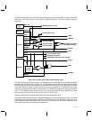
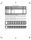
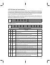
4.20 Wide-Band Data Registers
Bit 9 of the wide-band data register is the most recently received bit as shown below.
WBD
9–2 1–0
WBD
WB Data Reserved
R
WBDC l
9 8 7–5 4–0
WBDCtrl
WBD_LCKD WBD_ON WBD_BW Reserved
R/W
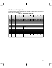
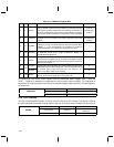
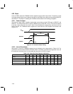
4.21 Base Station Offset Register
BST OFFSET values are 00, 01, 10, and 11, which correspond to an offset value d of 0, 1, 2, and 3
respectively as shown below.
BST OFFSET
9–2 1–0
BST OFFSET
Reserved Offset[1:0]
W
The delay in the TCM4300 TX channels is increased by the amount:
BST OFFSET
d
T
SINT
4