4–23
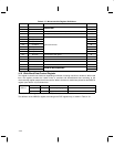
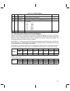
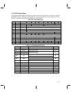
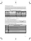
Table 4–18. WBDCtrl Register
BIT R/W NAME FUNCTION RESET VALUE
9 R/W WBD_LCKD
Wide-band data lock data. WBD_LCKD determines whether edge
detector is locked (1) or unlocked (0).
0
8 R/W WBD_ON Wide-band data on. WBD_ON turns the WBDD module on/off (1/0). 0
7–5 R/W WBD_BW[2:0] Wide-band data bandwidth. WBD_BW[2:0] sets the appropriate
PLL bandwidth.
000 : 20 Hz
001 : 39 Hz
010 : 78 Hz
011 : 156 Hz
100 : 313 Hz
101 : 625 Hz
110 : 1250 Hz
110
4–0 — — Reserved —
4.17 Microcontroller Status and Control Registers
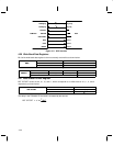
MCClock: This location is used by the microcontroller to change the speed of its own clock. The division
modulus is equal to a binary coded value written into this register. Only bits [5:0] are significant. After reset,
MCClock is equal to MCLKIN/32. Division moduli 2 through 32 are valid (0-1 moduli are prohibited). The
clock speed change occurs after the write is complete.
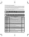
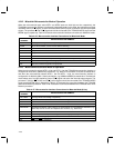
MIntCtrl Bits [7:4]: The bit names in this field indicate the resulting action when the bit is set to 1. When these
bits are being read, a 1 indicates that the corresponding interrupt is pending. A 0 indicates that the interrupt
is clear. Writing a 0 into any bit location has no effect.
MIntCtrl Bits [3:1]: These bits enable power to the AGC and AFC DACs and their corresponding outputs as
shown below. FMRXEN can assert (set to 1) the FMRXEN external function. The reset value is 0 (off).
MI C l
7 6 5 4 3 2 1 0
MIntCtrl
Clear
WBD
Clear-F Clear-D Send-C AGCEN AFCEN FMRXEN Reserved
R/W R/W R/W R/W R/W R/W R/W
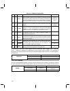
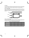
MStatCtrl: This register contains various signals needed for system monitoring and control as shown here
(also see Table 4–19).
MS C l
7 6 5 4 3 2 1 0
MStatCtrl
SYNOL TXONIND SYNRDY MCLKEN CVRDY AuxFS1 AuxFS0 MPAEN
R R R R/W R R/W R/W R/W


