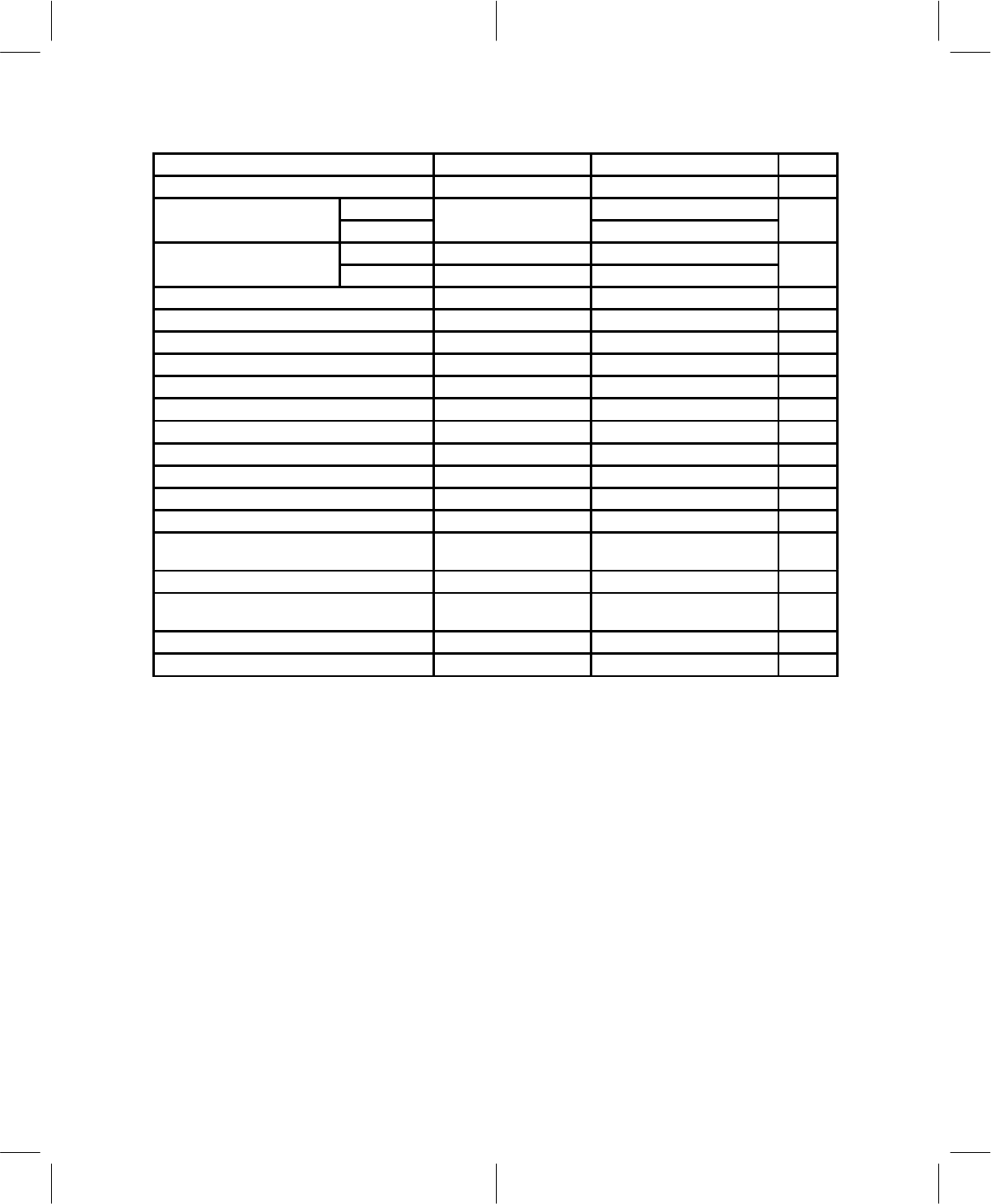
4–2
Table 4–2. RXIP, RXIN, RXQP, and RXQN Inputs (AV
DD
= 3 V, 4.5 V, 5 V)
PARAMETER TEST CONDITIONS MIN TYP MAX UNIT
Input voltage range 0.3 AV
DD
–0.3 V
Input voltage for full- scale
Differential 0.5
Input voltage for full scale
digital output
Single ended
0.5
p-p
Differential 0.125
om
na
opera
ng
eve
Single ended 0.125
Vp-p
Input CMRR (RXI, RXQ) 45 dB
Sampling frequency, SINT (digital mode) 48.6 kHz
Sampling frequency, SINT (analog mode) 40 kHz
Receive error vector magnitude (EVM) 5% 6%
I/Q sample timing skew Input signal 0 – 15 kHz 50 ns
A/D resolution 10 Bits
Signal to noise-plus distortion Input at full scale – 1 dB 54 58 dB
Integral nonlinearity 0 dB to –60 dB input 1 LSB
Gain error (I or Q channel) ±7%
Gain mismatch between I and Q ±0.3 dB
Differential dc offset voltage ±30 mV
FM input sensitivity, for full scale (±14 kHz
deviation)
2.5 Vp-p
FM input dc offset (wrt VHR) ±80 mV
FM input idle channel noise, below full scale
input
–50 dB
FM gain error ±6%
Power supply rejection f = 0 kHz to 15 kHz 40 dB
†
Provides 12 dB headroom for AGC fading conditions.
It is recommended that the single-ended output of an external FM discriminator be capacitively coupled to
the FM terminal for analog mode voice and WBD reception. An external bias resistor is needed to bias the
FM terminal to VHR. The signal at this terminal is conveyed to the Q side of the receiver using the multiplexer,
and the other Q input is connected internally to the VHR reference voltage. The I input of the receive section
circuitry is disabled in the analog mode. The FM signal passes through the antialiasing filter, as specified
in Table 4–3, before passing through the A/D converter. The signal at the FM terminal is also routed directly
to the WBD demodulator through a low-pass filter (LPF) with the –3 dB point at 270 kHz.


