


4–25
4.19 DSP Register Map
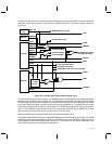
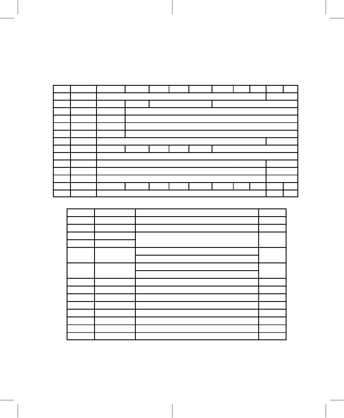
The register map accessible to the DSP port is shown in Table 4–20 and Table 4–21. There are 14 system
addressable locations. Note that the write address of FIFO B is the same as the read address of FIFO A.
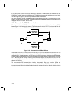
Figure 4-11 details the connection of TCM4300 to an example DSP.
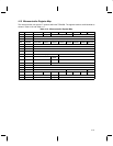
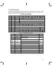
Table 4–20. DSP Register Map
ADDR NAME D9 D8 D7 D6 D5 D4 D3 D2 D1 D0
00h WBD MSB LSB Reserved
01h WBDCtrl WBD_LCKD WBD_ON WBD_BW Reserved
02h RXI Sign MSB LSB
03h RXQ Sign MSB LSB
04h TXI Sign MSB LSB
05h TXQ Sign MSB LSB
06h FIFO MSB FIFO A(B) microcontroller to DSP (DSP to microcontroller) LSB Reserved
07h DlntCtrl Clear WBD SDIS Clear-C Send-D Send-F Reserved
08h Timing Adj MSB LSB
09h AGC DAC MSB LSB Reserved
0Ah AFC DAC MSB LSB Reserved
0Bh PWR DAC MSB LSB Reserved
0Ch DStatCtrl TXGO MODE SCEN FMVOX FMRXEN IQRXEN TXEN OUT1 RXOF ALB
0Dh BST Offset Reserved MSB LSB
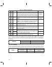
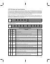
Table 4–21. DSP Register Definitions
ADDR NAME CATEGORY R/W
00h WBD Wide-band data R
01h WBDCtrl Wide-band data control R/W
02h RXI
RX channel A/D results
R
03h RXQ
RX
c
h
anne
l
A/D
resu
lt
s
R
04h
TXI
Analog mode: TXI D/A data
W
04h
TXI
Digital mode: π/4 DQPSK modulator input data
W
05h
TXQ
Analog mode: TXQ D/A data
W
05h
TXQ
Digital mode: Not used
W
06h FIFO FIFO A(B) microcontroller to DSP (DSP to microcontroller) R/(W)
07h DIntCtrl Interrupt control/status R/W
08h Timing Adj Symbol timing adjust W
09h AGC DAC AGC W
0Ah AFC DAC AFC W
0Bh PWR DAC Power control W
0Ch DStatCtrl Miscellaneous status/control R/W
0Dh BST Offset TDM burst offset W