4–11
4.9 Auxiliary DACs, LCD Contrast Converter (continued)
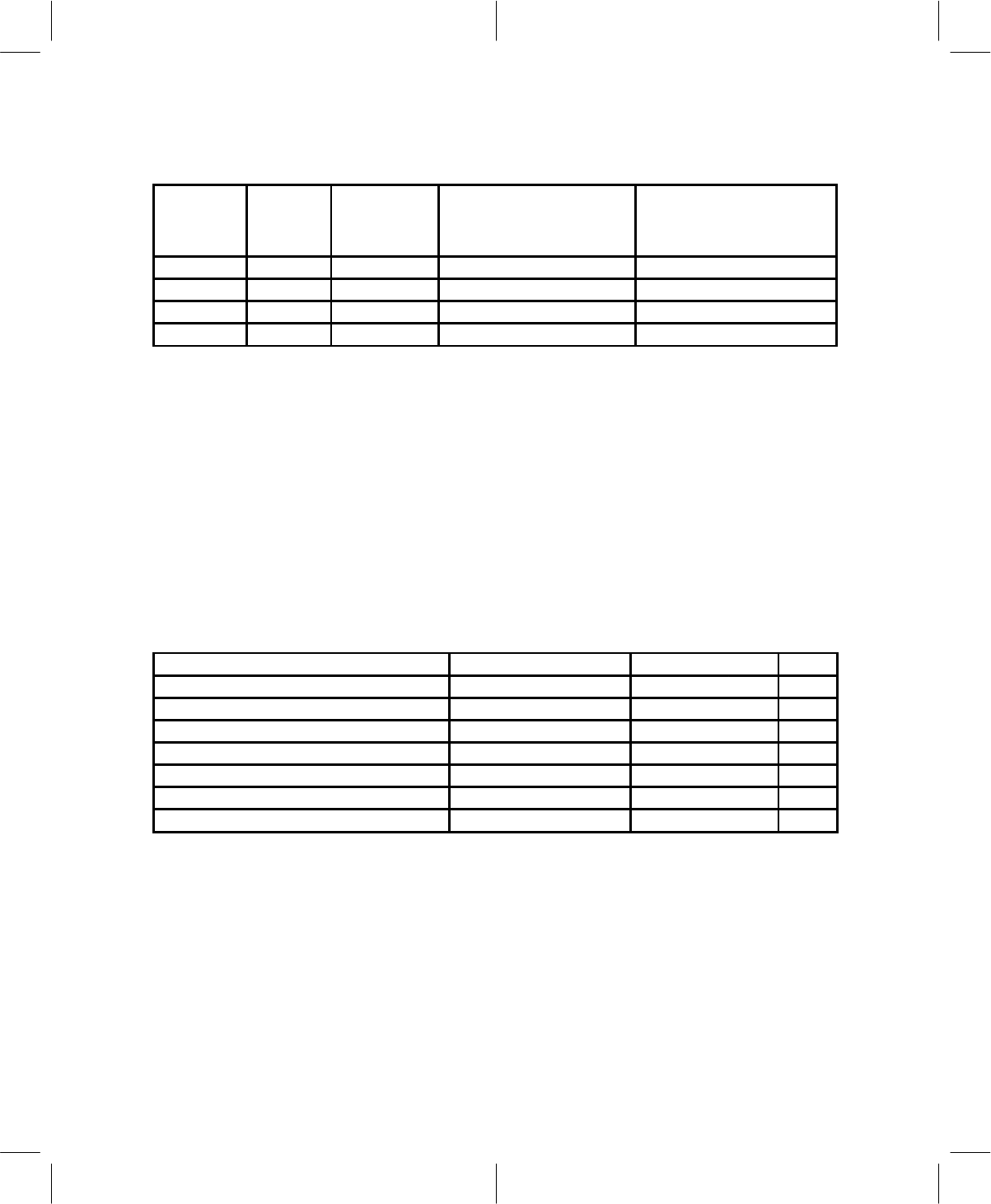
Table 4–12. Auxiliary D/A Converters Slope (LCDCONTR)
AUXFS[1:0]
SETTING
SLOPE
NOMINAL LSB
VALUE
(V)
NOMINAL OUTPUT VOLT-
AGE FOR DIGITAL CODE = 8
(MIDRANGE)
(V)
NOMINAL OUTPUT VOLTAGE
FOR DIGITAL CODE = 16†
(MAX VALUE)
(V)
00 2.5/16 0.1563 1.25 2.5
01 Do not use Do not use Do not use Do not use
10 4/16 0.2500 2 4
11 4.5/16 0.2813 2.25 4.5
†
The maximum input code is 15. The value shown for 16 is extrapolated.
4.10 RSSI, Battery Monitor
The received signal strength indicator (RSSI) and battery (BAT) strength monitor share a common register.
The input source is determined by writing any value to the mapped register location for that analog-to-digital
converter (ADC) (see Table 4–13), and the result of the conversion is stored in both register locations. The
conversion process is initiated when the register is written to. The CVRDY bit in the MStatCtrl register is set
to 1 to show completion of the conversion process. Reading from either of the register locations causes the
CVRDY bit to change to 0. The RSSI allows the mobile unit to choose the proper control channels and to
report signal levels to the base stations.
When the CVRDY bit in the MStatCtrl register goes to 1, this indicates that the latest RSSI or battery voltage
A/D conversion has been completed and can be read from the RSSI or BAT register location. CVRDY clears
to 0 when the microcontroller reads either of these locations.
Table 4–13. RSSI/Battery A/D Converter
PARAMETER TEST CONDITIONS MIN TYP MAX UNIT
Input range AV
DD
= 3 V, 4.5 V, 5 V 0.2 2 V
Resolution 8 bits
Conversion time AV
DD
= 3 V, 4.5 V, 5 V 20 µs
Gain + offset error (full scale) ±3% ±4%
Differential nonlinearity ±0.75 ±1 LSB
Integral nonlinearity ±0.75 ±1 LSB
Input resistance 1 2 MΩ
In order to save power, the entire RSSI/battery converter circuit is powered down when no A/D conversions
are requested for 40 µs. The microcontroller writes to RSSI or BAT registers, causing power to be applied
to the converter circuit. Power is applied to the converter circuit until the data value has been latched into
the corresponding register, at which time power to the converter is removed. Data remains in the result
registers after the converter is powered down.
4.11 Timing And Clock Generation
The digital timing generation system uses a 38.88-MHz master clock as shown in Figure 4–4. The upper
waveform shows the clock generation for clocks that must be phase adjusted in order to synchronize the
mobile unit with the received symbol stream in the digital mode. In the analog mode, these clocks operate
without phase adjustments. The bottom waveform of Figure 4–4 shows the clocks that are directly derived
from the master clock.


