


1–4
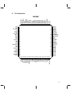
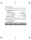
1.4 Terminal Functions
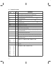
TERMINAL
I/O
DESCRIPTION
NAME NO.
I/O
DESCRIPTION
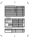
AFC 11 O Automatic frequency control. The AFC DAC output provides the means to adjust
system temperature-compensated reference oscillator (TCXO).
AGC 10 O Automatic gain control. The AGC digital-to-analog converter (DAC) output can be
used to control the gain of system receiver circuits.
AV
DD
REF 3 — Analog supply voltage for FM receive path. Power applied to AV
DD
REF powers the
FM receive path circuitry.
AV
DD
RX 7 — Analog supply voltage for receive path. Power applied to AV
DD
RX powers the receive
path circuitry.
AV
DD
TX 19 — Analog supply voltage for transmit path. Power applied to AV
DD
TX powers the
transmit path circuitry.
AV
SS
REF 98 — Analog ground for REFCAP
AV
SS
RX 12 — Analog ground for receive path
AV
SS
TX 22 — Analog ground for transmit path
BAT 1 I Battery strength monitor. A sample of the battery voltage is applied to BAT, and this
sample monitors the battery strength.
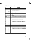
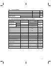
CINT 77 O Controller data interrupt. CINT is the microcontroller data interrupt (active low) signal
that is sent to the DSP. CINT is caused by a microcontroller write to the Send-C
interrupt register location.
CMCLK 92 O Codec master clock. CMCLK provides a 2.048-MHz clock that is used as the master
clock and bit clock for the speech codec.
CSCLK 93 O Codec sample clock. CSCLK provides an 8-kHz frame synchronization pulse for the
speech codec. CSCLK is also connected to the DSP for speech sample interrupts.
DINT 49 O Microcontroller interrupt request. DINT is output when the DSP writes to the SEND
DINT register location. DINT can be active high or low according to the levels of the
MTS0 and MTS1 signals.
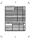
DSPA0 74
I DSP 4-bit parallel address bus. DSPA0 through DSPA3 provides the address bus for
th DSP i t f DSPA3 i th MSB d DSPA0 i th LSB
DSPA1 73
pgp
the DSP interface. DSPA3 is the MSB, and DSPA0 is the LSB.
DSPA2 72
DSPA3 71
DSPCSL 70 I DSP chip select (active low). A low signal at DSPCSL enables the specific DSP
addressed.
DSPD0 80
I/O/Z DSP 10-bit parallel data bus. DSPD0 through DSPD9 provide a 10-bit data bus for the
DSP DSPD9 i th MSB d DSPD0 i th LSB
DSPD1 81
pgp
DSP. DSPD9 is the MSB, and DSPD0 is the LSB.
DSPD2 82
DSPD3 83
DSPD4 84
DSPD5 85
DSPD6 86
DSPD7 87
DSPD8 88
DSPD9 89
†
Z = high impedance