4–10
4.9 Auxiliary DACs, LCD Contrast Converter
Auxiliary DACs generate AFC, AGC and power control signals for the RF system. These three D/A
converters are updated when the corresponding data is received from the DSP. In fewer than 5 µs after the
corresponding registers are written to, the output has settled to within 1 LSB of its new value (see
Table 4–10).
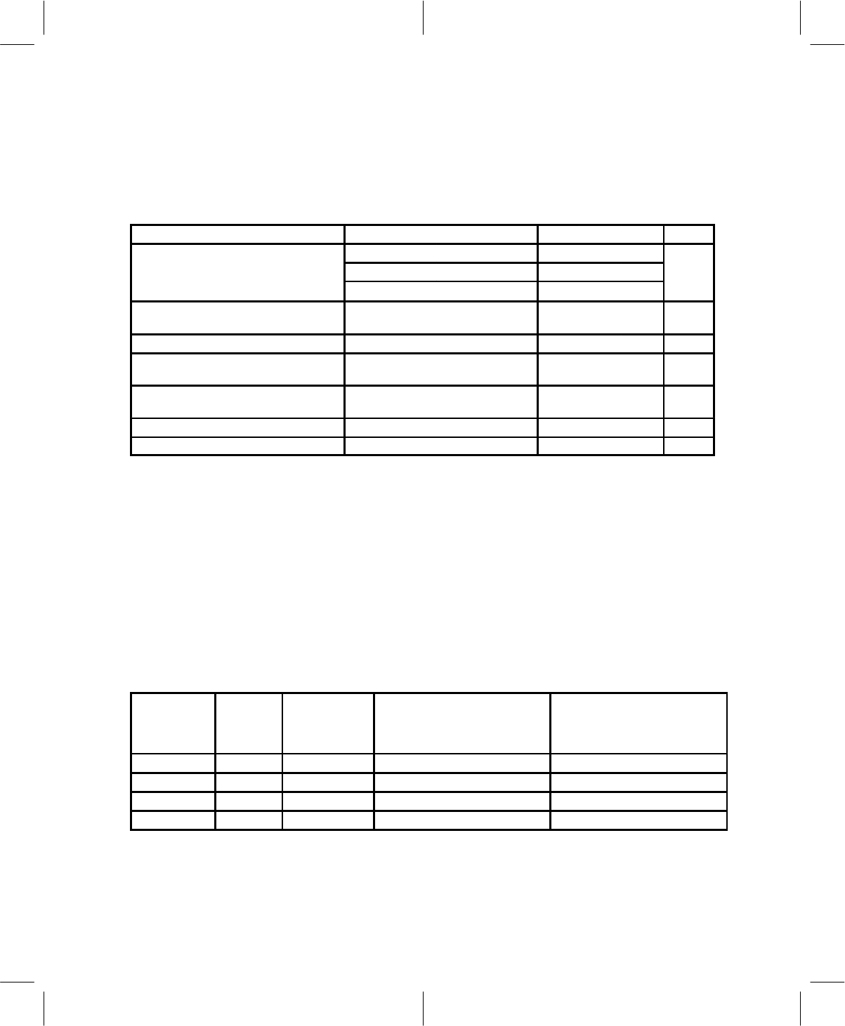
Table 4–10. Auxiliary D/A Converters
PARAMETER TEST CONDITIONS MIN TYP MAX UNIT
AV
DD
> 3 V
†
, AUXFS [1:0] = 00 0.2 2.5
Output range
AV
DD
> 4.5 V
†
, AUXFS [1:0] = 10 0.2 4
V
AV
DD
> 5 V
†
, AUXFS [1:0] = 11 0.2 4.5
Resolution AGC, AFC, PWRCONT
DACs
8 bits
Resolution LCDCONTR DAC 4 bits
Gain + offset error (full scale) AGC,
AFC, PWRCONT DAC
±3%
Gain + offset error (full scale)
LCDCONTR DAC
±7%
Differential nonlinearity ±0.75 ±1 LSB
Integral nonlinearity ±0.75 ±1 LSB
†
Range settings depends only on AUXFS [1:0]. The supply voltage is not detected.
The LCDCONTR output is used by the microcontroller to adjust the contrast of the liquid-crystal display
(LCD). This converter is a separate 4-bit DAC.
The auxiliary DACs can be powered down. The AGC and AFC DACs have dedicated bits in the MIntCtrl
register to enable the DACs. The PWRCONT DAC is enabled by the TXEN bit in the DStatCtrl register. The
LCDCONTR DAC is enabled when the LCDEN bit of the LCD D/A register clears to 0, the four data bits being
left justified. The AFC, AGC, and PWRCONT DACs are disabled after powerup or after a reset of the
TCM4300. After power up or reset, the default AUXFS[1:0] is 00. When the DACs are powered down, their
output terminals go to a high-impedance state and can tolerate any voltage present on the terminal that falls
within the supply range.
The slope and the corresponding output values for the auxiliary DACs are listed in Table 4–11 and
Table 4–12.
Table 4–11. Auxiliary D/A Converters Slope (AGC, AFC, PWRCONT)
AUXFS[1:0]
SETTING
SLOPE
NOMINAL LSB
VALUE
(V)
NOMINAL OUTPUT VOLTAGE
FOR DIGITAL CODE = 128
(MIDRANGE)
(V)
NOMINAL OUTPUT VOLTAGE
FOR DIGITAL CODE = 256
‡
(MAX VALUE)
(V)
00 2.5/256 0.0098 1.25 2.5
01 Do not use Do not use Do not use Do not use
10 4/256 0.0156 2 4
11 4.5/256 0.0176 2.25 4.5
‡
The maximum input code is 255. The value shown for 256 is extrapolated.
