


4–4
square-root raised-cosine (SQRC) shaping filter with a roll-off rate of α = 0.35 and converted to sampled
analog form by two 9-bit digital-to-analog converters (DACs). The output of the DAC is then filtered by a
continuous-time resistance-capacitance (RC) filter.
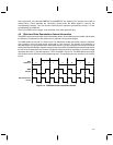
The TCM4300 generates a power amplifier (PA) control signal, PAEN, to enable the power supply for the
PA. The start and stop times of the TDM burst are controlled by writing to a single bit, TXGO, in the DSP
DStatCtrl register.
In the analog mode (MODE = 0), the DSP writes 8-bit I and Q samples into the TXI and TXQ data registers
at a 40-ksps rate. These writes are timed by the SINT interrupt signal. The samples are fed to a low-pass
filter before D/A conversion. In the transmit analog mode, PAEN is always set to 1.
The transmit section provides differential I and Q outputs (see Table 4-5) for both analog and digital modes.
The differential dc offset for the TXI and TXQ outputs can be independently adjusted using the transmit offset
registers.
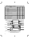
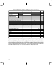
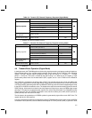
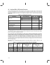
Table 4–5. Transmit (TX) I and Q Channel Outputs
PARAMETER MIN TYP MAX UNIT
Peak output voltage full scale centered at VCM
Differential 2.24
Vp
P
ea
k
ou
t
pu
t
vo
lt
age
f
u
ll
sca
l
e, cen
t
ere
d
a
t
VCM
Single ended 1.12
V
p
Nominal output-level (constellation radius) centered at
Differential 1.5
V
Nominal output level (constellation radius) centered at
VCM
Single ended 0.75
V
Low-level drift ±200 PPM/°C
Transmit error vector magnitude (EVM) 3% 4%
Resolution 8 bits
S/(N+D) ratio at differential outputs 48 52 dB
Gain error (I or Q channel) ±8% ±12%
Gain mismatch between I and Q ±0.3 dB
Gain sampling mismatch between I and Q 20 ns
Zero code error differential ±80 mV
Zero code error, each output, with respect to VCM ±80 mV
Zero code error, I to Q, with respect to other channel (differential or
single ended)
±10 mV
Load impedance, between P and N terminals 10 kΩ
Transmit offset DACs I and Q resolution 6 bits
Transmit offset DACs I and Q average step size 2.9 3.4 3.9 mV
Transmit offset DACs I and Q full-scale positive output 105.4 mV
Transmit offset DACs I and Q full-scale negative output –108.8 mV
Transmit offset DACs differential nonlinearity ±1.1 LSB
Transmit offset DACs integral nonlinearity ±1.1 LSB
Modulation Error: In the digital mode, during the transmit burst, the complex output of the transmitter circuits
consists of an ideal output s = I
ideal
+ jQ
ideal
+ error e = e
i
+ je
q
. In Table 4-5, the modulation error vector
magnitude (EVM) is defined as the peak value of the magnitude of e relative to the ideal output:
Modulation error percentage 100
|e|
|s|
%
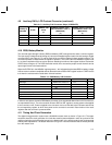
Table 4–6 and Table 4–7 show the frequency response of the transmit section for digital and analog mode,
respectively.