4–7
DQ
CLK
Dibit
In
TXGO
DQ
CLK
SINT
BST Offset
Delay
Channel Delay
(15.5 SINT Periods)
TXI,
TXQ
BST Offset
Delay
PAEN Delay
PAEN
Delay = 0, 1/4, 1/2, 3/4
Transmit Channel Delay + d(T/8)
Occurs from last symbol (2 SINT periods)
before TXGO goes low
PAEN Delay + d(T/8)
TXGO high: 9.5 SINT periods + d(T/8): PAEN high
TXGO low: 19.5 SINT periods + d(T/8): PAEN low
SYNOL
MPAEN
19.5
9.5
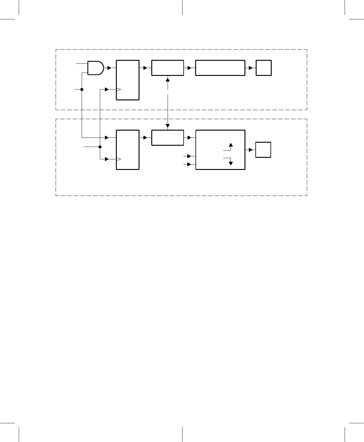
Figure 4–2. Transmit Power Ramp-Up/Ramp-Down Functional Diagram
4.5 Transmit I And Q Output Level
In the digital mode, the output level at TXI and TXQ is controlled by the TCM4300. During the burst, but not
including ramp-up or ramp-down periods, the average output level (I
2
+ Q
2
)
1/2
should approximate the
specified value. There is no variable level control for TXI and TXQ within the TCM4300 other than the fixed
ramping. In the analog mode, the output of the TCM4300 depends only on the sample values written to the
TXI and TXQ registers.
There are small differences in the average output power levels between the digital and the analog modes.
These differences require compensation at the system level by a small attenuation in the sample values of
the analog output.
When a change in transmit power is necessary, the microcontroller can change the value sent to the
PWRCONT DAC, the output of which can be connected to a voltage-controlled attenuator in the transmit
path of the RF section.
4.6 Wide-Band Data Demodulator
The wide-band data demodulator (WBDD) module demodulates the FM signal and outputs a
Manchester-decoded data stream. The WBDD is used for receiving the analog control channels of the
forward control channel (FOCC) and the forward voice channel (FVC). The bit error rate (BER) performance
requirements are listed in Table 4–8.


