


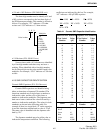

CIRCUIT DESCRIPTION
3-30
February 2001
Part No. 001-9800-001
RF chokes L502 and L503, ferrite bead EP502, and
several capacitors isolate the power control circuit
from RF signals.
A 50-ohm, 3 dB pad formed by R529-R531
provides an output impedance of 50 ohms at the J602.
Impedance matching between Q507 and this pad is
provided by two sections of microstrip, C524, and
C527. Power output at J602 is typically up to 250
milliwatts.
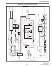
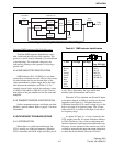
3.12.2 POWER AMPLIFIER MODULE (U600),
FINAL (Q651)
Power amplifier module U600 on the PA board
has approximately 19 dB of gain. Pins 2, 3, and 4 of
U600 are the supply voltage inputs to three separate
gain stages. The supply voltage on pin 2 (VS1) is
switched by Q600 and limited to 12 volts by CR601
and R600. Switch Q600 is controlled by the same
signal used to control 8V transmit switch Q505/Q504
(see Section 3.12.1).
The supply voltage applied to pins 3 and 4 (VS2/
VS3) is the unswitched battery from the power jack
fed through R601. Therefore, power is applied to these
pins of U800 even when transceiver power is turned
off. The power control circuit senses transmitter
current by monitoring the voltage drop across R601.
The output signal on U600, pin 5 is then applied
to Q651 (30 watt models only). With lower power
models, Q651 is not used. Amplifier Q651 provides
approximately 5 dB of gain. The output impedance on
U600, pin 5 is 50 ohms, and it is matched to Q651 by a
section of microstrip, C651, C652, and C653. Class C
bias of Q651 is provided by L651. The unswitched
battery supply applied to Q651 is isolated from RF by
L602, EP601, and several capacitors. Impedance
matching is provided on the output by C654-C656,
C614, and two sections of microstrip.
3.12.3 ANTENNA SWITCH
The antenna switch circuit consists of Q602,
CR602, CR604, several other components, and also a
quarter-wave section of microstrip and CR200 on the
RF board. This circuit switches the antenna to the
receiver in the receive mode and the transmitter in the
transmit mode.
Switching transistor Q602 is controlled by the
transmit signal from the Q7 output (pin 11) of shift
register U801. This is the same signal that controls
transmit 8-volt supply switch Q505/Q504. This signal
is high in the transmit mode and low in the receive
mode. Therefore, Q602 turns on in the transmit mode
and current flows from the collector of Q601 through
R610, R609, CR604, L604, CR602/R602, and L602.
In addition, 8 volts is applied through R200 to CR200
located at the input of the receiver on the RF board.
CR200, CR602 and CR604 are PIN diodes like
CR901 described in Section 3.10.2. When a PIN diode
is forward biased, it presents a very low impedance.
Therefore, in the transmit mode the transmit signal has
a low-impedance path to the antenna through CR602
and coupling capacitor C621.
The signal is blocked from the receiver by two
grounded quarter-wave lines. A discrete quarter-wave
line is formed by C635, C622, and L604 is effectively
AC grounded on the receiver end by CR604 and C633.
When one end of a quarter-wave line is grounded, the
other end presents a high impedance to the quarter-
wave frequency. Therefore, this line presents a high
impedance into the receiver for the transmit signal.
Further receiver isolation is provided by another
quarter-wave line in the receiver. This line is grounded
through C202 by CR200.
In the receive mode, all three PIN diodes are
reverse biased. Therefore, CR602 presents a high
impedance into the transmitter for the receive signal,
and since the two quarter-wave lines into the receiver
are no longer grounded, there is a low-impedance path
into the receiver. L604 presents a low impedance
because it is no longer grounded by CR604, and the
quarter-wave line presents a low impedance because it
is no longer grounded by CR200. Resistors R602 and
R608 improve the isolation provided by CR602 and
CR604 when they reverse biased (receive mode).
3.12.4 DIRECTIONAL COUPLER, LOW-
PASS FILTER
A directional coupler is formed by adjacent
sections of microstrip near C621. The forward compo-
nent of output power is rectified by CR603 and devel-
800/900 MHz RECEIVER DESCRIPTION