


CIRCUIT DESCRIPTION
3-5
February 2001
Part No. 001-9800-001
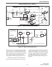
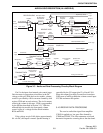
Address Bus
The address bus consisting of A0-A15 is used for
addressing the memory location in U107 or U108 that
data is being written to or read from. In addition, it
provides chip select signals to latches U110-U112.
Refer to Section 3.3.2 for more information on
memory and I/O addressing.
A/D Converter Inputs
VRH/VRL - These inputs provide the reference volt-
ages for the A/D converter circuitry. R115 and C105
attenuate noise present in the 5-volt supply applied to
VRH.
PE0 - RSSI (Receive Signal Strength Indicator) input
from limiter/detector U201 in the receiver. This signal
is used along with the squelch signal to determine
when valid data may be present and when to unmute
the receive audio.
PE1 - Battery voltage input. The switched 13.6-volt
supply is divided down by R161 and R168 to provide
a 0-5 volt input. If the battery voltage is excessively
high, the transmitter is disabled.
PE2 - Power amplifier temperature input from ther-
mistor R601 on the PA board. The DC voltage of this
signal decreases as temperature increases.
PE3 - Lock detect input from synthesizer IC U804. If
this signal is high (near 5 volts) the synthesizer is
locked on frequency (see Section 3.7.6).
PE4 - Power switch sense input. This input is high
when the power switch is on and low when it is off.
When the off condition is sensed, the microcontroller
saves the current settings and then powers down the
transceiver by turning Q110 off (see Section 3.2.1).
PE5 - Ignition switch sense input. This input is low
when the ignition switch is on and high when it is off.
The microcontroller senses the ignition switch to
control such features as the power-off delay and horn
alert.
PE6 - This input senses the voltage on the IN2 pin of
data modem connector J301 and Option 2 slot wire-out
W311.
PE7 - This input senses the voltage on the IN3 pin of
Option 1 slot wire-out W301.
Serial Peripheral Interface Port (SPI), OR Gate (U103)
This serial port is formed by the MOSI, MISO,
and SCK pins (31, 30, 32) of the microcontroller. It is
a synchronous port which means that a clock signal is
used to indicate when data on the data line is valid.
This port has both master and slave configurations and
in this application, the master configuration is always
used. In the master configuration the microcontroller
generates the clock and other signals.
MOSI (Master Out, Slave In) - This is the serial data
output for the port.
MISO (Master In, Slave Out) - This is the serial data
input for this port.
SCK - Serial clock output. This pin provides the clock
signal to all devices served by this port.
This port provides two-way serial data communi-
cation with EEPROM U102 (high tier and data
models) and microcontroller U2 on the display board
(high tier only). In addition, it provides programming
data to the RF board for shift registers U800 and
U801, digital potentiometer U802, and synthesizer IC
U804 (see Section 3.7.8). It also provides program-
ming data to shift register U305 (on the audio/logic
board) which controls the squelch level.
OR gates U103A-D provide routing of the serial
port signals to the RF and display boards. When the
PD5 output (pin 33) of the microcontroller goes low,
U103A and U103B route the data and clock signals to
the RF board and shift register U305. Then when the
Q4 output (pin 15) of latch U110 goes low, U103D
routes the clock signal to the display board and U103C
routes the display board data signal to the MISO pin.
When communicating with the display board, PD5
goes high to block the data path through U103A and
U103B.
Asynchronous Serial Communications Interface (SCI)
This is a full duplex serial port formed by the
RxD (data input) and TxD (data output) pins (28, 29)
of the microcontroller. This port uses a standard non-
AUDIO/LOGIC DESCRIPTION (ALL MODELS)