


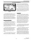

CIRCUIT DESCRIPTION
3-11
February 2001
Part No. 001-9800-001
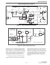
The functions controlled by U2 are as follows:
• Display controller U1 programming
• Backlight control
• Transmit/Busy indicator CR4 control
• Front panel option switch detection
• Front panel Select switch detection
• Microphone hanger off-hook detection.
The use of a separate microcontroller on the
display board minimizes the number of interconnec-
tions required with the audio/logic board because
separate lines are not required for each of the
preceding functions.
When the front panel Select switch is pressed, the
two PBNO lines are shorted together. Then when it is
rotated clockwise, low pulses appear on the CW line,
and when it is rotated counterclockwise, low pulses
appear on the CCW line. The contrast and viewing
angle of the display are set by potentiometer R46.
3.7 SYNTHESIZER CIRCUIT DESCRIPTION
(UHF MODELS)
3.7.1 INTRODUCTION
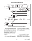
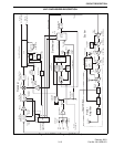
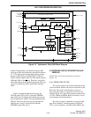
The synthesizer block diagram is part of the RF/
PA board diagram shown in Figure 3-4. The synthe-
sizer output signal is produced by a VCO (Voltage
Controlled Oscillator) located in a separate module
attached to the RF board. The frequency of the VCO is
controlled by a DC voltage from the phase detector in
synthesizer integrated circuit U804.
The phase detector senses the phase and
frequency difference between a highly stable signal
from the reference oscillator (fR) and a frequency
produced by dividing down the VCO signal (fV).
When the signal from the VCO is the same as the refer-
ence frequency, the VCO is on the correct frequency. If
the VCO-derived signal is not the same, the VCO
control voltage increases or decreases to change the
VCO frequency until they are the same. The VCO is
then “locked” on frequency.
The reference input (fR) to the phase detector is
produced by dividing down the signal from reference
oscillator U806. The fR input is 50 kHz for all UHF
channels. Therefore, the reference divider in U804
divides the 14.850 MHz reference oscillator signal by
297. The TCXO frequency stability is 2.0 PPM, so this
is also the stability of the synthesizer (and the second
injection signal which is derived from the TCXO
frequency).
The VCO-derived input to the phase detector (fV)
is the VCO frequency divided down by programmable
dividers in synthesizer U804. The prescaler and main
divider are programmed for each channel to produce
an input frequency to the phase detector (fV) that is
the same as the 50 kHz reference frequency (fR) when
the VCO is oscillating on the correct frequency. Refer
to Section 3.7.5 for more information on U804
operation.
3.7.2 VOLTAGE-CONTROLLED OSCILLATOR
Introduction
The VCO module is a separate assembly that is
soldered directly to the RF board and covered by a
metal shield. It uses a ceramic substrate that can easily
be damaged by excessive heat; therefore, it is recom-
mended that modules which have been removed using
a standard soldering iron not be reused. In addition, the
VCO center frequency is set by laser tuning ceramic
resonator L101. Therefore, it is not possible to adjust
this frequency if it changes as the result of changing a
part. For these reasons, the VCO is considered not field
serviceable.
Oscillator (Q102)
The VCO is formed by bipolar transistor Q102,
ceramic resonator L101, and several capacitors and
varactor diodes. It oscillates at the transmit frequency
in the transmit mode and 45 MHz below the receive
frequency in the receive mode (the first injection
frequency).
Biasing of Q102 is provided by R108 and R112,
and stabilization is provided by R114. Inductor L102
functions as an RF choke, and an AC voltage divider
formed by C112, C115, and C119 starts and maintains
oscillation and matches Q102 to the tank circuit.
The tank circuit consists of laser tuned inductor
L101, varactor diodes CR101, CR103-CR106, and
several capacitors. Inductor L101 is laser trimmed to
DISPLAY DESCRIPTION