CIRCUIT DESCRIPTION
3-27
February 2001
Part No. 001-9800-001
divide number. In this example the fractional-N incre-
ment is .75 x 8 (modulo N) or 6. This causes the pres-
caler to divide by 65 for one additional output pulse
for 6 of 8 main divider cycles. This produces a divide
number that is .75 higher. Therefore, with the
preceding example, the overall divide number K is 845
+ 15,424 + .75 or 16,269.75. The VCO frequency of
813.4875 MHz divided by 16,269.75 equals 50 kHz
which is the fR input to the phase detector.
NOTE: The formulas for calculating the “N” and “A”
divide numbers are described in Section 4.3.5.
3.10.7 LOCK DETECT
When the synthesizer is locked on frequency, the
LOCK output of U804 (pin 18) is a logic high voltage.
Then when the synthesizer is unlocked, this voltage is
low. A locked condition exists when the phase differ-
ence at the TCXO input is less than one cycle.
3.10.8 CHARGE PUMP
The charge pump circuit in U804 charges and
discharges C833-C837 in the loop filter to produce the
VCO control voltage. Resistors connected to the RN
and RF pins set the charge current. The RF pin resis-
tance is set by a digitally controlled potentiometer in
U802. This resistance changes with the frequency
band in order to minimize fractional-N spurious
signals. The loop filter provides low-pass filtering
which controls synthesizer stability and lockup time
and suppresses the loop reference frequency (50 kHz).
3.10.9 SHIFT REGISTER (U800, U801) AND
DIGITAL POTENTIOMETER (U802)
PROGRAMMING
Shift register U800 functions as an I/O port
expander, and shift register U801 functions as a D/A
converter to provide a 256-step output voltage for
adjusting transmitter power. In addition, the Q7 output
of U801 provides the delayed transmit signal. U802
contains four digitally controlled potentiometers that
are adjustable in 256 steps.
These devices are cascaded together on the serial
bus so that data is shifted out of one device into
another. Programming is performed using the SPI
serial port of the microcontroller described in Section
3.3.1. The input to the internal shift register of these
devices is the DATA (U800/U801) or SDI (U802) pin,
and the output of the last shift register stage in U800
and U801 is the QS
pin. Therefore, serial data on the
Data line from the audio/logic board (J201, pin 14) is
first shifted into U801, then U800, and then U802.
Data is clocked through the devices by the
CLOCK signal (J201, pin 13) when the STROBE
input (J201, pin 12) is high and latched when it goes
low. Synthesizer IC U804 is also programmed by the
SPI port. However, data does not pass through the
other devices because it is controlled by a different
STROBE signal (J201, pin 1).
3.11 RECEIVER CIRCUIT DESCRIPTION
(800/900 MHz MODELS)
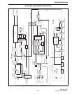
NOTE: The receiver block diagram is in Figure 3-7.
3.11.1 FRONT END FILTER
The receive signal is fed from the antenna switch
circuit on the PA board to the receiver front end on the
RF board. The signal is fed through a quarter-wave
line that is part of the antenna switch as are C202,
CR200, and R200. Refer to Section 3.12.3 for more
antenna switch information. The receive signal is then
applied to bandpass filter Z200. With 800 MHz
models, this is a three-pole filter with a center
frequency of 860 MHz and a bandwidth of 18 MHz.
With 900 MHz models, it is a two-pole filter with a
center frequency of 938 MHz and a bandwidth of 6
MHz. This filter attenuates frequencies outside the
receive band such as the first injection, image, and half
IF frequencies.
3.11.2 RF AMPLIFIER (Q201)
RF amplifier Q201 improves and stabilizes
receiver sensitivity and also recovers filter losses. A
section of microstrip and C214 provide impedance
matching on the input. CR203 protects the base-
emitter junction of Q201 from damage caused by high
level input signals.
The bias current of Q201 is fixed at a constant
level by Q200. The collector current of Q201 flows
through R207, and the voltage drop across that resistor
(and therefore the current) is set by R205 and R206.
800/900 MHz SYNTHESIZER DESCRIPTION


