


CIRCUIT DESCRIPTION
3-25
February 2001
Part No. 001-9800-001
cially at the lower audio frequencies. Conversely, if
only the reference oscillator was modulated, the VCO
frequency would not change fast enough, especially at
the higher audio frequencies. By modulating both, a
relatively flat response is provided for all modulation
frequencies.
Separate audio, data, and wideband data modula-
tion signals are applied to the synthesizer on J201, pins
18, 17, and 16, respectively. The data signal includes
LTR and Call Guard signaling, and the wideband data
signal (if used) comes directly from an external device
such as a modem and does not pass through the
limiting and filtering circuitry.
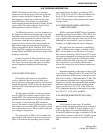
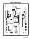
The levels of the audio and data signals are set by
digitally controlled variable resistors in U802. These
resistors are adjusted in 256 steps by serial data from
the microcontroller (see Section 3.3.1). The transmit
audio signal is applied to pins 2 and 4 which are the
wiper and one end of a potentiometer. It is fed out on
pin 3 which is the other end of the potentiometer (see
Figure 3-7). Likewise, the data signal is fed in on pins
22 and 24 and out on pin 23. These variable resistors
set the modulation level of the audio and data signals
and also allow the microcontroller to provide
frequency compensation. This compensation is
required because modulation tends to increase as the
VCO frequency increases (tank circuit capacitance
decreases).
The output signals on pin 23 and 3 are then
combined with the wideband data signal and applied to
summing amplifier U803. The output signal from
U803 is then applied to the reference oscillator on pin
1 and also across the potentiometer connected to pin
19 of U802. The output on pin 18 is applied to the
VCO on pin 5. This modulates both the reference
oscillator and VCO. The resistor across pins 19 and 18
of U802 adjusts the balance of these signals.
3.10.4 ACTIVE FILTER (Q800)
Q800 functions as a capacitance multiplier to
provide a filtered 7.0-volt supply to the VCO. Resistor
R827 provides bias, and C814 provides the capacitance
that is multiplied. CR800 decreases the time required
to charge C814 when power is turned on. If a noise
pulse or other voltage change appears on the collector,
the base voltage does not change significantly because
of C814. Therefore, base current does not change and
the voltage on the emitter remains constant.
3.10.5 BUFFER AMPLIFIER (Q801), TX/TX
SWITCH (CR801/CR802)
The output signal on pin 2 of the VCO is applied
to buffer amplifier Q801. Impedance matching on the
input is provided by C822, a section of microstrip, and
C826. Microstrip is a form of transmission line with
distributed series inductance and shunt capacitance.
The characteristic impedance is determined by the
width of the microstrip and the PC board material and
thickness (distance from ground plane). This stage
provides isolation and also amplifies the signal to
produce an output level of approximately 0 dBm.
The bias current of Q801 is fixed at a constant
level by Q802. The collector current of Q801 flows
through R830. The voltage drop across that resistor
(and therefore the current) is set by R836 and R837.
For example, if current through R830 attempts to
increase, the emitter voltage of Q802 decreases. Q802
then conducts less and turns Q801 off slightly to main-
tain a constant bias current. This provides a stable bias
over changes in temperature.
Capacitors C813, C817, C827, and C844
decouple RF signals, and a section of microstrip and
C818 provide impedance matching with the transmit/
receive switch. R832 lowers the Q of the microstrip to
make it less frequency selective.
The transmit/receive switch formed by CR801,
CR802, and several other components switches the
VCO signal to the receiver in the receive mode and the
transmitter in the transmit mode. CR801 and CR802
are PIN diodes similar to CR901 described in Section
3.10.2. Therefore, they present a very low impedance
when forward biased and a very high impedance when
reverse biased.
These diodes are controlled by the Q2 signal from
shift register U800. This signal is high in the transmit
mode and low in the receive mode. Therefore, when
the transmitter is keyed, both Q805 and Q806 turn on
and CR801 and CR802 are forward biased by the
current flowing through Q806, R856, L800, CR801,
CR802, R857, and Q805.
800/900 MHz SYNTHESIZER DESCRIPTION