


CIRCUIT DESCRIPTION
3-29
February 2001
Part No. 001-9800-001
If a narrowband channel is selected, a low signal
is applied to the base of Q205. That transistor is then
turned off and inverter Q206 turned on. CR209/CR210
are then forward biased and CR207/CR208 reverse
biased. This routes the 450 kHz IF signal through
Z202 and blocks it from Z206. If a wideband channel
is selected, the opposite occurs. For more information
on the operation of PIN diodes, refer to Section 3.11.1.
The filtered 450 MHz IF signal is then applied to
pin 18, amplified by an internal amplifier, and fed
back out on pin 16 and applied to ceramic filter Z205.
This filter is identical to Z206 and provides additional
attenuation of wideband noise. The loss introduced by
each ceramic filter is approximately 12 dB.
Limiter/Detector
The signal from Z205 is applied to an internal
limiter connected to pin 14. The limiter amplifies the
450 kHz signal and then limits it to a specific value to
remove amplitude variations. From the limiter, the
signal is fed internally to the quadrature detector. An
external phase shift network connected to pin 10 shifts
the phase of one of the detector input signals 90° at
450 kHz (the other input is unshifted in phase). When
modulation occurs, the frequency of the IF signal
changes at an audio rate as does the phase of the
shifted signal. The detector, which has no output with
a 90° phase shift, converts this phase shift into an
audio signal. L218 is tuned to provide maximum
undistorted output from the detector.
The audio signal is then fed internally to an audio
amplifier. The gain of this stage is set at about three by
R255 and R256. The audio signal is then fed out on
pin 8 and routed to the audio/logic board.
Also in U201 is an RSSI detector which provides
a temperature compensated RSSI (Receive Signal
Strength Indicator) signal on pin 5. This is a low
impedance (2k ohm) output with a dynamic range of
70 dB. The DC voltage of this output changes in
proportion to IF signal strength. This signal is routed
to an A/D input of the microcontroller (pin 59) and
used along with the squelch signal to determine
receive signal strength. R259/C304 and R258/C303
provide low pass filtering of the audio and RSSI
signals, and C305 and C306 decouple RF.
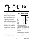
3.12 TRANSMITTER CIRCUIT DESCRIPTION
(800/900 MHz MODELS)
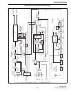
NOTE: The transmitter block diagram is located in
Figure 3-7.
3.12.1 PREDRIVER (Q506), DRIVER (Q507)
The input signal to the exciter is the transmit
frequency from buffer amplifier Q801 in the synthe-
sizer. It is at a level of approximately 0 dBm and is
applied to predriver Q506. Impedance matching on the
input of Q506 is provided by C529, C515, two
sections of microstrip (see description in Section
3.10.5), R518, and C516. Biasing is provided by
R519, R520, R522, and R523. Various AC signals are
decoupled from the DC supply by C520, C525, C526,
C528, and C531.
The 8-volt supply voltage to this stage is switched
on in the transmit mode by Q505 and Q504. This
switch is controlled by the microcontroller through the
Q7 output (pin 11) of shift register U801. This output
is high in the transmit mode and low in the receive
mode. This signal also controls the antenna switch
circuit on the PA board described in Section 3.12.3.
This transmit 8V supply is not delayed which
allows Q505 and the transmitter frequency to stabilize
before power is produced. The delayed PTT signal is
applied to the RF board on J201, pin 2. This signal
controls the power control circuit described in Section
3.12.5. The emitters of Q503 and Q505 are grounded
through Q509. That transistor is turned off when the
logic is in an undetermined state such as during Flash
programming. This ensures that the transmitter is
turned off during these times.
From Q506 the transmit RF output signal is then
applied to driver Q507. Impedance matching between
Q506 and Q507 is provided by several capacitors and
sections of microstrip and L501. Resistor R521 lowers
the Q of the parallel microstrip which makes it less
frequency selective. Q507 is biased for class C opera-
tion by L504 and ferrite bead EP501.
Supply voltage to Q507 is from the power control
circuit described in Section 3.12.5. This circuit varies
the supply voltage of Q507 which changes its power
output to maintain constant transmitter power output.
800/900 MHz TRANSMITTER DESCRIPTION