FAULT FINDING
SECTION 100-816-500
MARCH 1993
-2-
3.06 The following precautions must be observed
when handling PCBs:
DO NOT:
Drop a PCB.
Stack one PCB on top of another.
Handle a PCB without discharging any
static electricity from your person by
touching the grounded cabinet.
Touch PCB contacts with your fingers.
Important!
If the fault is not cleared by substituting a
PCB, the original PCB must be reinstalled
in the KSU before trying another PCB.
4 DEFECTIVE APPARATUS RETURNS
4.01 When a defective system apparatus is
shipped for repair, the apparatus must be packed
in a suitable container (the original box is highly
recommended), as follows:
a) Anti-static containers for all other PCBs and
Feature cartridge.
b) Plastic bags for digital or electronic tele-
phones, KSU, etc.
4.02 NEVER WRITE ON THE APPARATUS
ITSELF! Describe the nature of the defect on an
information tag. Attach the tag to the front of the
unit with string (not wire) so the tag can remain
attached during the testing and repair process.
Return tags are available from Toshiba America
Information Systems, Inc., TSD Division.
5 FAULT IDENTIFICATION AND
ELIMINATION PROCEDURES
5.01 The DK8 or DK16, KSU common control
circuits or DK16 KFCU may contain a “soft” fault
due to an extremely high level of static electricity.
If it is found defective during the fault finding
procedures, attempt to clear a soft fault prior to
returning the KSU or KFCU for repair. The
correct procedure for this is to perform the
initialization procedure, and then re-program
the system as necessary to test for the fault. If
the fault returns after these procedures are
performed, tag the defective KSU or KFCU and
return it for repair.
6 DK8 HARDWARE FAULT ISOLATION
6.01 If a DK8 hardware fault is suspected, check
the hardware using the following procedure:
1) Make sure the BATT jumper plug (SW1 on the
KSU motherboard) is in the ON position to
save the system’s customer data base.
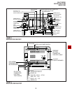
2) Unplug HPFB battery cable from BATT con-
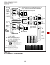
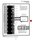
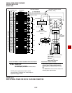
nector on QPSU8 Power Supply (see Figure
2).
3) Remove all piggy-back PCBs from the DK8
motherboard one at a time. Retest to check if
the problem is cleared each time a PCB is
removed. If it is found that a particular PCB is
causing the problem, replace that PCB and
retest (piggy-back PCBs include QSTU,
QCDU, QRCU, QCNU, and QSMU).
4) Test power supply as follows (refer to Figure
2):
a) Plug the AC power cable into an outlet.
The “AC” LED on the power supply
should light green.
b) Turn the power supply switch to the ON
position.
The “DC” LED on the power supply
should light green.
c) Using the voltmeter, measure the volt-
ages referenced to frame ground (FG) at
the power supply connector CN3 pins
(test points) and pin 42 of IC5 located on
the motherboard (Figure 2). The volt-
ages should fall within the ranges below.
If the voltages do not fall within the
range, unplug the DC power pins from
power supply connector CN3 and mea-
sure +24V again at the same location; if
the voltages remain unacceptable, re-
place the power supply (see Section
100-816-204).
J19 Green Wires: 0V
J19 Yellow Wires: +24V
Range: +26.3V ~ +27.8V
IC5, Pin 42, +5V
Range: +4.5V ~ +5.5V
d) If the +24V tests within range but +5V is
not with-in specification, the KSU must
be replaced.


