


4 - 6
The passed signals are then applied to the RF amplifier cir-
cuit.
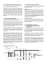
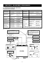
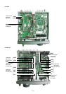
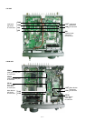
4-4-2 1200 MHz RF CIRCUIT (for RX)
Received signals from the transmit/receive switching circuit
are passed through the high-pass filter (L285–L287, L289,
C297–C300) and pre-amplifier (Q281) and are applied to the
RF amplifier circuit (Q271) via the band pass filter circuit
(FI281).
The amplified signals are then passed through the another
bandpass filter (FI271) to suppress unwanted signals. The
filtered signals are then applied to the 1st mixer circuit
(IC241).
4-4-3 1200 MHz 1ST/2ND MIXER CIRCUITS (for RX)
The 1st/2nd mixer circuits convert the received signals into
a fixed frequency of the 10 MHz IF signal with a PLL output
frequencies. By changing the PLL frequency, only the
desired frequency will pass through a filter at the next stage.
The filtered signals from the bandpass filter are mixed with
1st LO signals at the mixer circuit (IC241) to produce a 1st
IF signal (243.95 MHz). The 1st LO signals (996.0
MHz–1076.1 MHz) are PLL output frequency, which comes
from the 1st LO VCO circuit (Q451, Q452).
The 1st IF signal is passed through the bandpass filter
(FI241) to suppress unwanted signals, and then applied to
the 2nd mixer circuit (Q221).
The applied signal is mixed with 2nd LO signal coming from
the 2nd LO VCO circuit (Q731) to produce a 10.85 MHz
[Main], 10.95 MHz [Sub] 2nd IF signal. The 2nd IF signal is
passed through the main/sub switching circuit (Q161,
Q164), and then output to the MAIN unit of IC-910H via J311
(pin 25 [Main], pin 1 [Sub]).
4-4-4 IF AMPLIFIER CIRCUIT (for TX)
The modulated 2nd IF signal from IC-910H via J311 is ampli-
fied at the 2nd IF amplifier (Q81), and is passed through the
low-pass filter (L82, L83, C80, C85–C89) to suppress
unwanted signals. The filtered signal is then applied to the
2nd mixer circuit.
The applied signal is mixed at the 2nd mixer circuit (D82,
L84, L85) to converted into the 1st LO signal with the 2nd LO
signal, which comes from the 2nd LO VCO (Q731).
Then the 1st LO signal is passed through the low-pass filter
(L121, L122, C121–C125) and amplified at the 1st IF ampli-
fier (IC111). The amplified signal is passed through the
bandpass filter (FI101) between the attenuators
(R104–R106) and (R133–R135), and are then applied to the
1st mixer circuit (IC131).
The signal is mixed with the 1st LO signal coming from the
1st LO VCO circuit (Q451, Q452) to converted into RF sig-
nals.
4-4-5 DRIVE/POWER AMPLIFIER CIRCUITS (for TX)
The RF signals from the 1st mixer circuit are passed through
the bandpass filter (FI141) and low-pass filter (L141, L142,
C142–C146), and then amplified at the YGR amplifier circuit
(IC141).
The amplified signals are passed through the bandpass fil-
ter (FI1) to suppress spurious components, and are ampli-
fied at the pre-drive amplifier (Q36, Q38) and power module
(IC21) to obtain a stable 10 W of output power.
The output signals from the power module (IC21) are
passed through the duplexer circuit (RL51) and detector cir-
cuits of forwared voltage and refrected voltage, and are then
applied to the antenna connector.
4-4-6 PLL CIRCUITS
UX-910 contains 2 frequency synthesizer circuit. This unit
does not have a local oscillator circuit and uses a 30.2 MHz
frequency from IC-910H as a reference frequency. The 2nd
LO circuit adopt “Icom’s original I-loop PLL” to obtain 1 Hz
pitch fine tuning.
The reference frequency from the IC-910H via J312 is
amplified at the reference amplifier (IC601, Q601) and
applied to the 2LO DDS IC (IC661). A portion of the refer-
ence signal is also applied to the divider circuit (IC610). The
divided signal is applied to the 1LO PLL circuit (IC501).
4-4-7 1LO PLL CIRCUIT
The 1LO PLL circuit generates the 1st LO frequency, and
the signal is applied to the 1st mixer circuit as the “1LO” sig-
nal.
An oscillated signal from the 1LO VCO (Q541, Q542) pass-
es through the buffer amplifiers (Q551, Q681) and is applied
to the PLL IC (IC501, pin 1) and is prescaled in the PLL IC
based on the divided ratio (N-data). The reference signal is
also applied to the PLL IC (IC501, pin 6). The PLL IC detects
the out-of-step phase using the reference frequency and
outputs it from pin 10. The output signal is passed through
the active filter (IC502, Q511, Q512) and is then applied to
the 1LO VCO circuit as the lock voltage.
4-4-8 2LO PLL CIRCUIT
The 2LO PLL circuit generates the 2nd LO frequency, and
the signal is applied to the 2nd mixer circuit as the “2LO” sig-
nal.
The signal generated at the 2LO VCO circuit (Q731) is
amplified at the buffer amplifiers (Q741, Q761), then applied
to the prescaler circuit (IC761). The prescaler circuit divides
the applied signal, and outputs it to the DDS circuit (IC661)
via the buffer amplifier (Q762). The DDS circuit generates
digital signals using the applied signals as a clock frequen-
cy. The phase detector section in IC661 compares its phase
with the reference frequency from the reference amplifier
(IC601). IC661 outputs off-phase components as pulse sig-
nals via pins 51, 52.
The output pulses are converted into DC voltage at the loop
filter circuit (IC701a) and then applied to the 2LO VCO cir-
cuit.
The D/A converter (R621–R645), low-pass filter
(L651–L653, C651–C657) and buffer amplifier (IC621) cir-
cuits are connected to the DDS output to convert the digital
oscillated signals into smooth analog signals.