


4 - 4
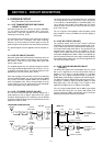
While in SSB mode, the amplified signals from the buffer
amplifier (Q1651) are then applied to the balanced modula-
tor (IC201).
While in AM/FM mode, the amplified signals from the buffer
amplifier (Q1651) are applied to the limiter amplifier
(IC1651b) and splatter filter (IC1651a). The signals are
passed through the buffer amplifier ((IC1652a) and are then
applied to the AM detector (IC1807d, D1652) in AM mode or
to the varactor diode (D253) in FM mode.
4-2-2 MODULATION CIRCUIT (MAIN UNIT)
(1) FM mode
The amplified audio signals from IC1701 are pre-empha-
sized and limited at IC1651b and then passed through the
splatter filter (IC1651a). The filtered signals are then applied
to the FM modulation circuit (D253) via the FM deviation
level controller (IC1803 pins 21, 22) and buffer amplifier
(IC1652a). Also, subaudible tone signals from the CPU
(DISPLAY board; IC1 pin 4) are applied to the FM modula-
tion circuit (D253) via the splatter filter (IC1651a).
The FM modulation circuit changes the generating frequen-
cy of the FM local oscillator (Q254, X251) to generate an FM
signal. The modulated IF signal is passed through the RF
limiter (Q253) and then applied to the transmit IF amplifier
circuit.
When 9600 bps mode is selected, audio signals from the
ACC connector bypass the amplifiers and are applied to
IC1654a directly via the external modulation switch (IC1531,
pins 12, 1). In such cases, the deviation detector (IC1807d)
cuts off the audio line when over modulation is detected.
(2) SSB and CW modes
The amplified audio signals from Q1651 are mixed with BFO
signals at the balanced mixer circuit (IC201) to produce a 10
MHz IF signal. The mixed signal is still a DSB signal, there-
fore, the mixed signal passes through bandpass filter circuit
(FI151) to suppress unwanted side band signals. The fil-
tered signal is applied to the transmit IF amplifier circuit
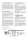
4-2-3 CW KEYING CIRCUIT (MAIN UNIT)
When the CW key is closed, control signal is output from
CPU (LOGIC unit) and controls break-in operation, the side
tone signal.
Keying signals (DOT and DASH) from the [KEY] jack
(J1401) are applied to the CPU (DISPLAY board; IC1, pins
49, 48 respectively), and the CPU outputs a CW control sig-
nal (KDS1) from pin 21. The CW control signal is applied to
the balanced mixer (IC201) via Q201, D201, D207 to unbal-
ance the IC201 input bias voltage and creates a carrier sig-
nal. R202 determines the transmit delay timing.
4-2-4 TRANSMIT IF AMPLIFIER CIRCUIT
(MAIN UNIT)
The modulated IF signal from a modulation circuit is applied
to the IF amplifier circuit (Q1). The amplified IF signal is then
applied to the VHF/UHF transmit circuit (PA unit) via the VHF
/UHF switching circuit (D52, D53).
The gain of the IF amplifier circuit (Q1) is controlled by the
ALC amplifier circuit (IC1601b). Therefore, the IF amplifier
is reduced when the output power increases.
4-2-5 RF CIRCUIT (PA UNIT)
The RF circuit consists of mixer and drive amplifiers to
obtain the desired frequency and level needed at a PA cir-
cuit, respectively.
(1) VHF band
The IF signal from the MAIN unit (P501) is mixed with an LO
signal from the VHF VCO circuit (PLL unit; Q191,
D191–D194) at the double-balanced mixer circuit (Q501,
Q502, D502) to be converted into VHF transmit frequency.
The mixed signal is passed through the attenuator
(R512–R514) and two-stage tunable bandpass filter (D503,
L533 and D504, L504) to suppress spurious components.
The filtered signals are then amplified at the YGR amplifier
(IC501) and passed through the attenuator (R562–R531)
and another two-stage tunable bandpass filter (D641, L641
and D642, L642)
The amplified and filtered RF signal is applied to the drive
amplifier circuit that is used VHF and UHF signals common-
ly.
(2) UHF band
The IF signal from the MAIN unit (P1) is mixed with a 2nd LO
signal at the double-balanced mixer circuit (Q1, Q2) to pro-
duce a 2nd IF signal (71.25 MHz). The 2nd LO signal (60.4
MHz) is generated at the reference oscillator and doubler
circuit (PLL unit; X512, Q551) via LO amplifier (IC40). The
2nd IF signal is amplified at the buffer amplifier (Q3) via the
bandpass filter circuit (L3, L4, C12, C13, C15–C17, C24,
C26). The amplified 2nd IF signal is applied to the 1st mixer
circuit (D190, L190, L191) passing through the attenuator
(R12–R14) and low-pass filter (L381, L382, C381–C383).
The 1st mixer circuit (D190, L190, L191) converts the 2nd IF
signal into a UHF transmit frequency with a 1st LO signal
from the UHF VCO circuit (PLL unit; Q391, D391–D394).
The converted RF signal is passed through the bandpass fil-
ter (FI200 and FI201) where unwanted LO signal emission
is reduced. The filtered signal is attenuated at R204–R206
and amplified at the YGR amplifier (IC200), and is then
applied to the drive amplifier circuit via the band pass filter
(FI202) and another YGR amplifier (Q200).
4-2-6 DRIVE AMPLIFIER CIRCUIT (PA UNIT)
The drive amplifier circuit amplifies RF signals from the VHF
or UHF RF circuit to obtain a level needed at the power
amplifier circuit. One drive amplifier circuit is commonly used
for both VHF and UHF band signals.
The signals from the VHF or UHF RF circuit are amplified at
the drive amplifier circuit (Q101, Q121, Q131, DRV board;
Q930). The amplified VHF signals are passed through the
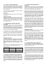
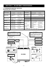
• Transmit IF frequencies
Mode Transmit IF signal
USB
LSB
CW
10.8485 MHz
10.8515 MHz
10.8491 MHz