


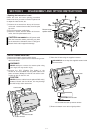

SECTION 4 CIRCUIT DESCRIPTION
4 - 1
4-1 RECEIVER CIRCUIT
Note: [Main]=Main band, [Sub]=Sub band
4-1-1 VHF TRANSMIT/RECEIVE SWITCHING
CIRCUIT (PA UNIT)
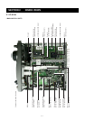
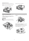
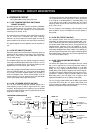
Received signals from the antenna connector (CHASSIS;
J1) are passed through the low-pass filter (L723–L721,
C728–C726, C728) then applied to the transmit/receive
switching circuit (RL700, D710).
The transmit/receive switching circuit leads receive signal to
the RF circuit from a low-pass filter while receiving.
However, the circuit leads the transmit signal from the RF
power amplifier to the antenna connector while transmitting.
The passed signals are then applied to the RF amplifier cir-
cuit.
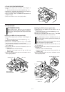
4-1-2 VHF RF CIRCUIT (PA UNIT)
Received signals from transmit/receive switching circuit are
applied to the RF amplifier circuit (Q507) via the RF attenu-
ator (D515), limiter (D514) and tunable band pass filter
(D513, L560) circuits.
The amplified signals are then passed through the another
three-stage tunable bandpass filters (D512–D510, L13–L15)
to suppress unwanted signals. The filtered signals are then
applied to the 1st mixer circuit (Q511, Q512).
D510–D513 employ varactor diodes, which are controlled by
the CPU (DISPLAY board; IC1) via the D/A converter (MAIN
unit; IC1521) and buffer amplifier (MAIN unit; IC1522d), to
track the bandpass filter. These varactor diodes tune the
center frequency of an RF pass band for wide bandwidth
receiving and good image response rejection.
4-1-3 VHF 1ST MIXER CIRCUIT (PA UNIT)
The 1st mixer circuit converts the received signals into a
fixed frequency of the 10 MHz IF signal with a PLL output
frequency. By changing the PLL frequency, only the desired
frequency will pass through a pair of crystal filters at the next
stage of the VHF 1st mixer.
The filtered signals from the bandpass filter are mixed with
1st LO signals at the mixer circuit (Q511, Q512) to produce
a 1st IF signal (10.85 MHz [Main] or 10.95 MHz [Sub]). The
1st LO signals (125.15 MHz–163.15 MHz) are PLL output
frequency, which comes from the VHF VCO circuit (PLL unit;
Q191, D191–D194).
The 1st IF signal is then applied to either the Main or Sub
band 10 MHz IF circuit in the MAIN unit via P501 [Main] or
P510 [Sub].
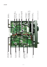
4-1-4 UHF RF CIRCUIT (PA UNIT)
The received signals from the UHF antenna connector
(CHASSIS; J2) are passed through the low-pass filter (L181,
L180, C188–C184) and then transmit/receive switching cir-
cuit (D182–D185, D265, D266, D227). The signals from the
transmit/receive switching circuit are applied to the RF
amplifier circuit (Q260) via the RF attenuator circuit (D264)
and tunable bandpass filter (D263, L288). The amplified sig-
nals are passed through the three-stage tunable bandpass
filters (D262–D260, L262–L260), and are then applied to the
1st mixer circuit (Q220, Q221).
4-1-5 UHF 1ST AND 2ND MIXER CIRCUIT
(PA UNIT)
The filtered RF signals from the bandpass filter are mixed
with a 1st LO signal at the 1st mixer circuit (Q220, Q221) to
produce a 1st IF signal (71.25 MHz [Main] or 71.35 MHz
[Sub]). The 1st IF signal is passed through a crystal filter
(Fl280 [Main], Fl281 [Sub]) to suppress out-of-band signals.
The filtered IF signal is applied to the 2nd mixer circuit (Q11)
to produce a 10 MHz IF signal (10.85 MHz [Main] or 10.95
MHz [Sub]) with a 2nd LO signal. The IF signal is then
applied to the MAIN unit via P1 [Main] or P30 [Sub].
The 1st LO signal (348.75 MHz–408.75 MHz) is generated
at the UHF VCO circuit (PLL unit; Q391, D391–D394), and
a 2nd LO signal (60.2 MHz) is produced at the PLL circuit by
doubling it’s reference frequency (30.2 MHz).
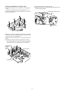
• RECEIVER CONSTRUCTION
430 MHz
1st mixer
Q220, Q221
1st LO
B1LO
2nd mixer
Q11
AF signals to
AF selector circuit
(IC452)
2nd LO
B2LO
LPF BPF BPF BPF
BPF
IC351FI51 FI151
BFOM
to FM IF IC (IC401)
BPF
144 MHz
1st mixer
Q511, Q512
1st LO
A1LO
AF signals to
AF selector circuit
(IC1002)
LPF
BPF BPF
IC851FI651 FI751
BFOM
to FM IF IC (IC951)
BPF
for MAIN band
for SUB band
10.95 MHz
10.85 MHz
MAIN unitPA unit