


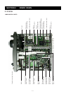
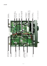
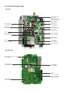

4 - 2
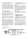
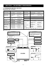
4-1-6 10 MHz IF CIRCUIT (MAIN UNIT)
The 10 MHz IF signal from the mixer circuit is passed
through a monolithic filter (Fl51 [Main], Fl651 [Sub]) to sup-
press out-of-band signals. The filtered signal is amplified at
the IF amplifier (Q51 [Main], Q651 [Sub]). The IF amplifier
provides 20 dB gain.
The amplified signal is then applied to the different circuits
depending on the selected mode.
(1) FM mode
The signal is applied to an FM IF IC pin 16 (IC401 [Main] or
IC951 [Sub]).
(2) SSB and CW mode
The signal is passed through a 10 MHz IF filter (FI151/10.85
MHz [Main] or Fl751/10.95 MHz [Sub]) or optional CW nar-
row filters. The filtered signal is amplified at the IF amplifiers
(Q350–Q352 [Main] or Q850–Q852 [Sub]) and then applied
to a demodulator circuit.
4-1-7 DEMODULATOR CIRCUIT (MAIN UNIT)
(1) FM mode
The 10 MHz IF signal from an IF amplifier (Q51 [Main] or
Q651 [Sub]) is applied to the mixer section of the FM IF IC
(IC401 [Main], IC951 [Sub], pin 16), and is mixed with a LO
signal (10.395 MHz [Main], 10.495 MHz [Sub]) to produce a
455 kHz IF signal. The LO signal is generated by the BFO
circuit (PLL unit; IC601 [Main], IC701 [Sub]).
The FM detector circuit employs the quadrature detection
method, which uses a ceramic discriminator (X401 [Main],
X951 [Sub]) for phase delay to obtain a non-adjusting circuit.
The detected signals are output from pin 9, and applied to
the squelch control and center indication detector circuits,
etc.
(2) SSB and CW modes
The amplified signal from the IF amplifier circuit (Q51 [Main],
Q651 [Sub]) is applied to the balanced mixer circuit (IC351
[Main], IC851 [Sub]) to demodulate into AF signals.
Demodulated audio signals are output from pin 1, and
applied to the squelch control gate (IC452 [Main], IC1002
[Sub]).
BFO circuit (PLL unit; IC601 [Main] and IC701 [Sub]) gener-
ates BFO signals for using in the balanced mixers.
4-1-8 SQUELCH CONTROL CIRCUIT (MAIN UNIT)
The demodulated AF signals from the balanced mixer circuit
or FM IF IC are applied to the squelch control gate (IC452
[Main], IC1002 [Sub]). This consists of 4 analog switches
which are selected with a mode signal and squelch control
signal from the CPU (DISPLAY board; IC1) via the expander
IC (IC1491). The switched AF signals are applied to the AF
circuit.
4-1-9 SQUELCH CIRCUIT (MAIN UNIT)
(1) FM mode
A squelch circuit cuts out AF signals when no RF signal is
received or the S-meter signal is lower than the [SQL] con-
trol setting level. By detecting noise components in the AF
signals, the CPU switches the squelch control gate.
A portion of the AF signals from the FM IF IC pin 9 (IC401
[Main], IC951 [Sub]) passes through the active filter section
of FM IFIC (pin 8). The active filter section amplifies and fil-
ters noise components. The filtered signals are applied to
the noise detector section for conversion into DC voltage
and output from pin 14 (IC401 [Main], IC951 [Sub]) as the
“NSQM [Main]/NSQS [Sub]” signal. The “NSQM [Main]/
NSQS [Sub]” signal is applied to the DISPLAY board.
The DC voltages are passed through the analog multiplexer
(DISPLAY board; IC5, pins 15 and 2) and then applied to the
CPU (DISPLAY board; IC1, pins 93, 94) via the MP1Y and
MP1X signal lines. The [SQL] level signal is also applied to
the CPU via the analog multiplexer (DISPLAY board; IC3,
pins 14, 5) as a reference voltage for comparison with the
noise signals. Also, an S-meter signal is applied to the CPU
from FM IF IC pin 12 (IC401 [Main], IC951 [Sub]) via the
meter amplifier (IC1804c [Main], IC1804a [Sub]) and analog
multiplexer (DISPLAY board; IC4, pins 12 and 1). The CPU
compares these signals, then outputs a control signals to
the squelch control gate.
(2) SSB and CW modes
The squelch circuit mutes audio output when the S-meter
signal is lower than the [SQL] control setting level.
A portion of the 10 MHz IF signal from the IF amplifier (Q352
[Main], Q852 [Sub]) is converted into DC voltage at the AGC
detector (D303, Q305 [Main], D902 Q901 [Sub]) and ampli-
fied at the meter amplifier (IC1804d [Main] or IC1804b
[Sub]). The amplified signal is passed through the analog
multiplexer (DISPLAY board; IC4, pins 12 and 1) via the
SMLM [Main]/ SMLS [Sub] signals and then applied to the
CPU (DISPLAY board; IC1). The CPU outputs control sig-
nals to the squelch control gate when the S-meter signal is
low level.
4-1-10 AF AMPLIFIER CIRCUIT (MAIN UNIT)
The AF amplifier circuit amplifiers the demodulated signals
to drive a speaker. For the separate speaker function, a
stereo power amplifier is used.
AF signals from the squelch control gate are passed through
the AF filter (IC451a [Main], IC1001a [Sub]) and AF pre-
amplifier (IC451b [Main], IC1001b [Sub]) and then amplified
at the voltage controlled amplifier (VCA: IC1808 [Main],
IC1809 [Sub]) which functions as a volume control using the
[AF] control signal. The amplified AF signals are applied to
the AF power amplifier circuit (IC1852, pin 2 [Main], pin 5
[Sub]).
The amplified audio signals of SUB band are output from pin
7, and are applied to the external speaker jack for the SUB
band (J1852) via the [PHONE] jack (JACK board; J1). When
no plug is connected to the jack, the signals are fed back to
the MAIN band audio. The mixed audio is applied to the
internal speaker via the [PHONE] jack and external speaker
jack for the MAIN band (J1851).
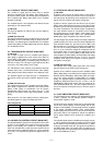
• BFO frequencies
Mode for MAIN band for SUB band
USB
LSB
CW
10.8485 MHz
10.8515 MHz
10.8483 MHz
10.9485 MHz
10.9515 MHz
10.9483 MHz