


错误!未知的文档属性名称
Hardware Guide
Mechanical Specifications
Issue 01 (2011-04-08)
Huawei Proprietary and Confidential
Copyright © Huawei Technologies Co., Ltd.
56
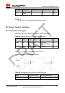
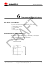
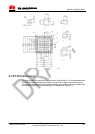
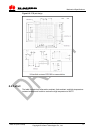
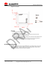
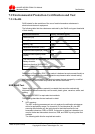
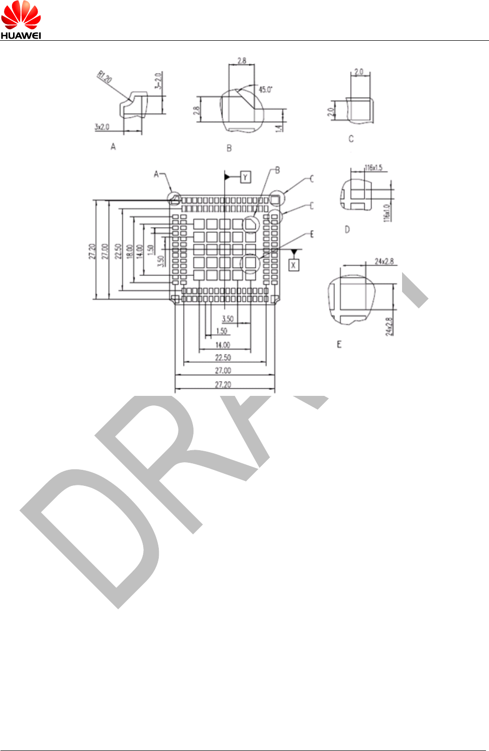
6.3 PCB Pad Design
To achieve assembly yields and solder joints of high reliability, it is recommended that
the PCB pad size be designed as follows: the size of the pad in the middle region is
the same as the pad size of the product package; other pads are 0.05 mm larger than
the unilateral pad of the product package. For details, see Figure 6-2 .