


HUAWEI MC509 CDMA LGA Module
Hardware Guide
Description of the Application Interfaces
Issue 01 (2011-04-08)
Huawei Proprietary and Confidential
Copyright © Huawei Technologies Co., Ltd.
23
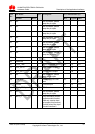
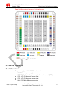
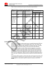
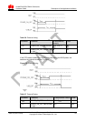
Table 3-2 lists the definitions of the pins on the power supply interface.
Table 3-2 Definitions of the pins on the power supply interface
Pin No.
Signal Name
I/O
Description
DC Characteristics (V)
Min
Typical
Max
12, 13
VBAT
P
Pins for power
voltage input
3.3
3.8
4.2
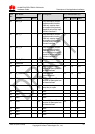
48, 49, 50,
52, 53, 54,
56, 57, 58,
59, 106,
108, 110,
112, 114,
116
GND
-
GND
-
-
-
35
VCOIN
P
Pin for standby
power input of
the RTC
1.5
3.0
3.25
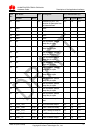
32
VCC_EXT1
P
Pin for external
power output
-
2.6
-
31
VCC_EXT2
P
Pin for external
power output
-
1.8
-
34
UIM_VCC
P
Power supply for
UIM card
-0.3
1.8/2.85
2.1/3.15
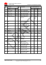
121~145
GND
-
Thermal Ground
Pad
-
-
-
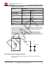
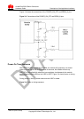
3.3.2 VBAT Interface
When the MC509 module works normally, power is supplied through the VBAT pins
and the voltage ranges from 3.3V to 4.2V (typical value: 3.8V). The 145-pin LGA
provides two VBAT pins and sixteen GND pins for external power input. To ensure
that the MC509 module works normally, all the pins must be used efficiently.
When the MC509 module is used for different external applications, pay special
attention to the design for the power supply. When the MC509 module transmits
signals at the maximum power, the transient current may reach the transient peak
value of about 1.5A due to the differences in actual network environments. In this
case, the VBAT voltage drops. Make sure that the voltage does not decrease below
3.3V in any case. Otherwise, exceptions such as restart of the MC509 module may
occur.
A low-dropout (LDO) regulator or switch power with current output of more than 1.5A
is recommended for external power supply. Furthermore, a 220uF or above energy
storage capacitor is connected in parallel at the power interface of the MC509
module.