


HUAWEI MC509 CDMA LGA Module
Hardware Guide
Description of the Application Interfaces
Issue 01 (2011-04-08)
Huawei Proprietary and Confidential
Copyright © Huawei Technologies Co., Ltd.
41
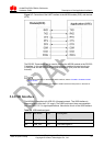
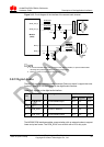
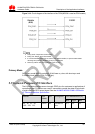
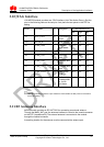
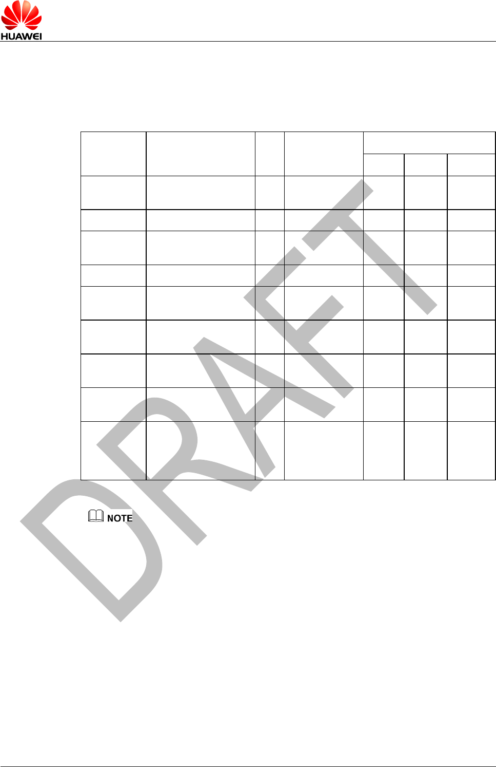
3.10 JTAG Interface
LGA MC509 module provides one JTAG interface (Joint Test Action Group). Set the
pins in the following table as the test pins. And place the test points in the DTE for
debug.
Pin No.
Pin Name
I/O
Description
DC Characteristics (V)
Min
Type
Max
31
VCC_EXT2
O
2.6V POWER
output
-
2.6
-
100
RESIN_N
I
Reset module
-0.3
1.8
2.1
30
JTAG_TMS
I
JTAG Test
mode select
-0.3
2.6
2.9
36
JTAG_TRST_N
I
JTAG reset.
-0.3
2.6
2.9
42
JTAG_TCK
I
JTAG clock
input
-0.3
2.6
2.9
72
JTAG_TDO
Z
JTAG test data
output
-0.3
2.6
2.9
87
JTAG_TDI
I
JTAG test data
input
-0.3
2.6
2.9
93
JTAG_RTCK
O
JTAG return
clock
-0.3
2.6
2.9
14
PS_HOLD
I
This input high
to keep power
on, low to
shut down.
-
1.8
-
It is recommended that set the 9 pins related to JTAG interface as test points on the DTE for
tracing and debug.
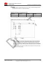
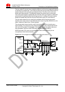
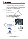
3.11 RF Antenna Interface
MC509 module provides an RF ANT PAD for connecting an external antenna.
Through the MAIN_ANT pad, the antenna interface is routed to the coaxial connector
on the DTE (Impedance 50).The external antenna is connected to the module
through the coaxial connector.
A matching location for the antenna must be reserved at the antenna port.