


HUAWEI MC509 CDMA LGA Module
Hardware Guide
Description of the Application Interfaces
Issue 01 (2011-04-08)
Huawei Proprietary and Confidential
Copyright © Huawei Technologies Co., Ltd.
40
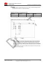
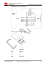
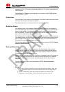
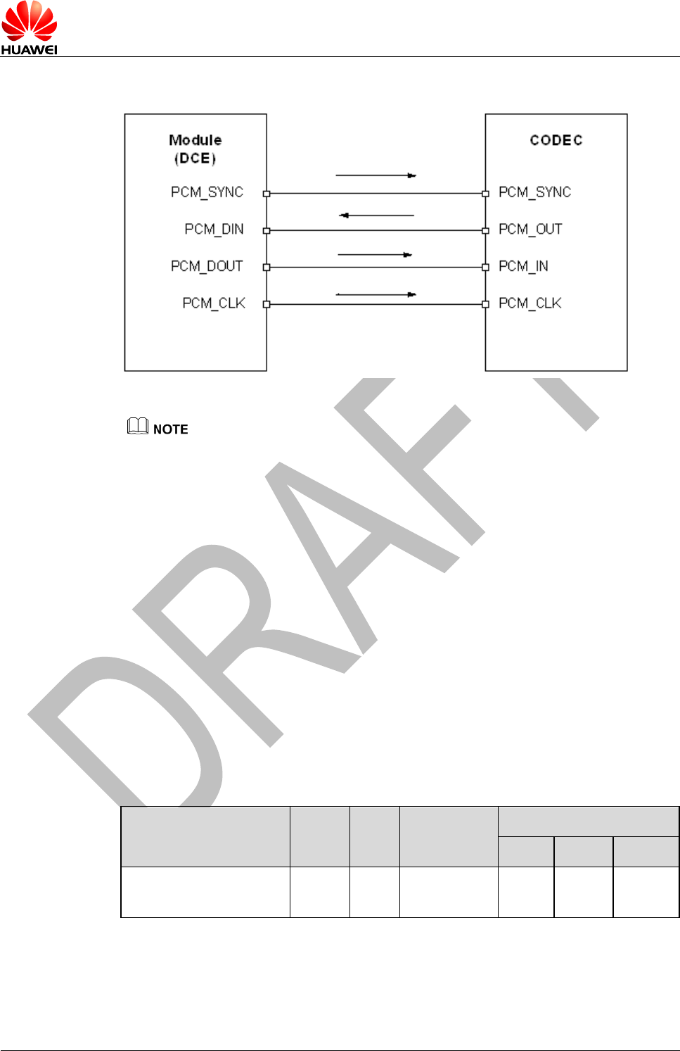
Figure 3-14 Circuit diagram of the interface of the PCM (MC509 is used as PCM master)
PCM_SYNC: Output when PCM master
PCM_CLK: Output when PCM master
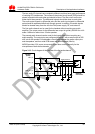
It is recommended that a TVS be used on the related interface, to prevent electrostatic
discharge and protect integrated circuit (IC) components.
Data only edition does not support the voice function.
Primary Mode
On Primary mode MU509 provides a 16-bit linear or μ-law, with short-sync and
2.048MHz clock (on the PCM_CLOCK pin).
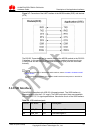
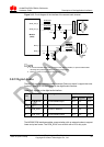
3.9 General Purpose I/O Interface
The LGA module provides seven channels GPIO pins for customers to applications of
controlling signal. Customers can use AT command to control the state of logic levels
of eight channels GPIO output signal. See the HUAWEI MC509 CDMA LGA Module
AT Command Interface Specification.
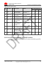
Pin No.
Pin
Name
I/O
Description
DC Characteristics (V)
Min
Type
Max
44,46,51,55,
105,109,113,
GPIO
I/O
General I/O
pins
-0.3
2.6
2.9