


CIRCUIT DESCRIPTION
3-16
February 2001
Part No. 001-9800-001
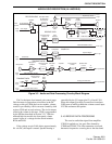
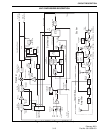
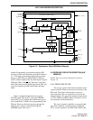
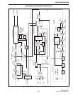
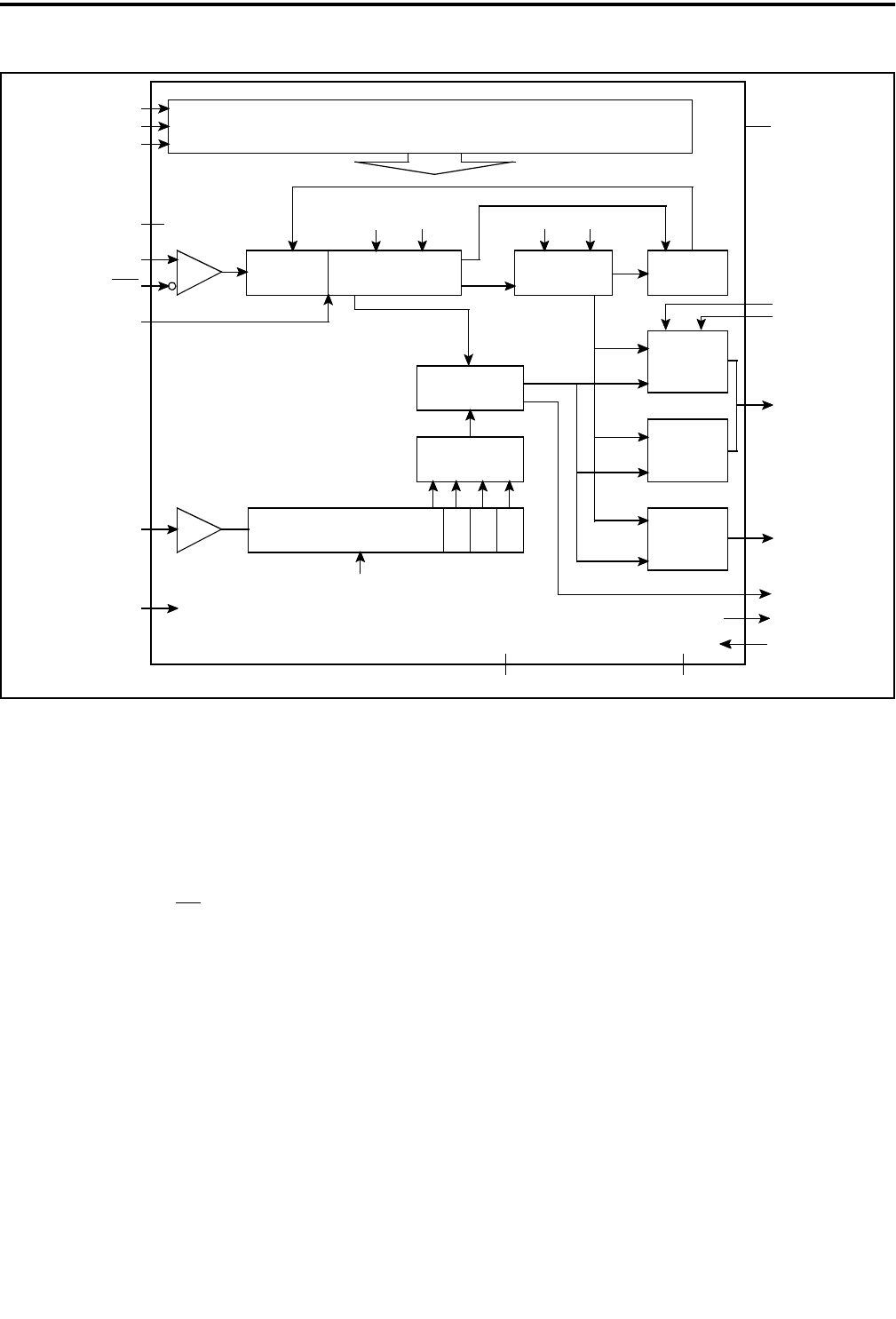
Figure 3-5 Synthesizer Chip U804 Block Diagram
(1) CLOCK
(2) DATA
(3) STROBE
(4, 12) Vss
(5) RF
IN
(6) RF
IN
÷64/65
Prescaler
Main Dividers
Fractional
Accumulator
Prescaler
Modulus
Control
FMOD
Serial Input + Program Latches
V
DD (7, 15, 20)
(19) TEST
IN
(8) REF
Reference Divider
÷2 ÷2 ÷2
Main
Main
Phase
Detector
Reference
Select
IN
(10) AUX
Normal
Output
Charge
Pump
Output
Charge
Pump
Speed-Up
Output
Charge
Pump
Integral
V
SSA
V
DDA
LOCK (18)
PHA (11)
RA (9)
PHI (13)
PHP (14)
RN (16)
RF (17)
f
V
f
R
÷N
÷A
F INC
÷R
another. Programming is performed using the SPI
serial port of the microcontroller described in Section
3.3.1. The input to the internal shift register of these
devices is the DATA pin (U800/U801) or SDI pin
(U802), and the output of the last shift register stage in
U800 and U801 is the QS
pin. Therefore, serial data
on the Data line from the audio/logic board (J201, pin
14) is first shifted into U801, then U800, and then
U802.
Data is clocked through the devices by the
CLOCK signal (J201, pin 13) when the STROBE
input (J201, pin 12) is high and latched when it goes
low. Synthesizer IC U804 is also programmed by the
SPI port. However, data does not pass through the
other devices, and it is controlled by different
STROBE signal (J201, pin 1).
3.8 RECEIVER CIRCUIT DESCRIPTION (UHF
MODELS)
NOTE: The receiver block diagram is shown in
Figure 3-4.
3.8.1 FRONT END FILTER
The receive signal is fed from the antenna switch
circuit on the PA board to the receiver front end on the
RF board. The signal is fed through a section of
microstrip that is part of a quarter-wave line for the
antenna switch. Also part of the antenna switch circuit
is C201, CR200, and R200. Refer to Section 3.9.4 for
more antenna switch information.
The receive signal is applied to a two-pole band-
pass filter formed by ceramic resonators L200 and
L201, several capacitors, and PIN diodes CR201 and
UHF SYNTHESIZER DESCRIPTION