TK-8180
17
2-5. Squelch Circuit
The output signal from IC172 enters FM IC again, then
passed through a band-pass filter.
The noise component output from IC172 is amplified by
Q175 and rectified by D173 to produce a DC Voltage corre-
sponding to the noise level. The DC voltage is sent to the
analog port of the CPU (IC404).
IC172 outputs a DC voltage (RSSI) corresponding to the
input of the IF amplifier.
3. Transmitter Circuit
The transmitter circuit consists of the following circuits : 3-
1 microphone circuit, 3-2 modulation level adjustment circuit,
3-3 driver and final power amplifier circuit, and 3-4 automatic
power control circuit.
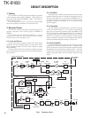
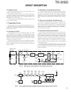
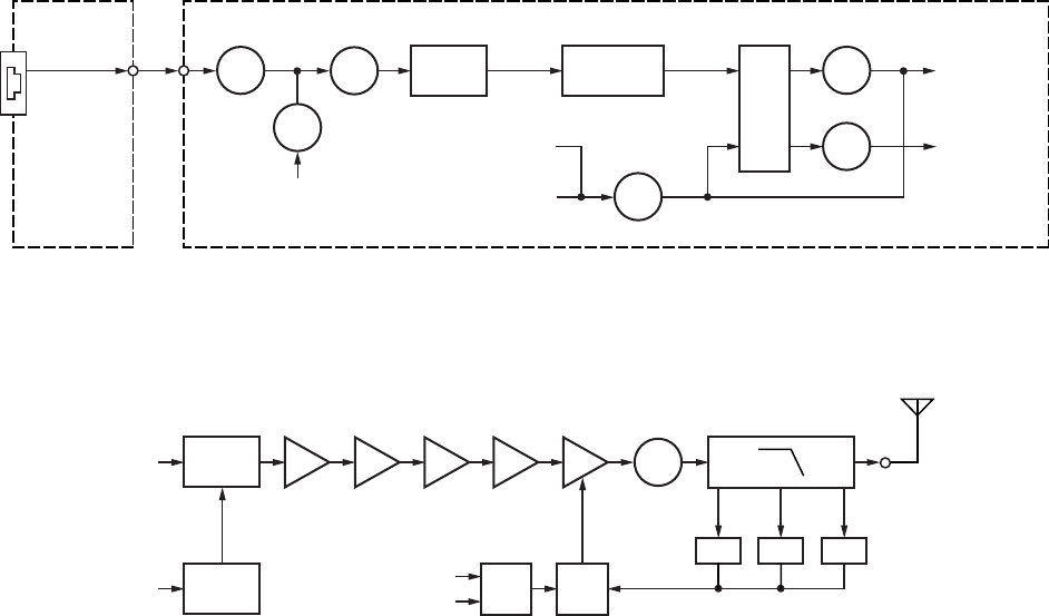
3-1. Microphone Circuit
The audio signal from the microphone goes into TX-RX
unit (X57-699) from the display unit (X54-348) and passes
through the mute switch (Q416). The audio signal is ampli-
fied by the microphone amplifier (IC414) and is input into the
TXIN terminal of the audio processor (IC415) after passing
through the multiplexer (IC413).
The input audio signal is output from the MOD terminal of
the audio processor (IC415) and is amplified by the audio fre-
quency amplifier (IC412) after passing through the electric
volume (IC410).
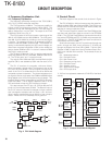
3-2. Modulation Level Adjustment Circuit
The audio signal amplified by the audio frequency ampli-
fier (IC412) is added to the low speed data LSD passed
through the low pass filter (IC409). The combined signals is
supplied to the VCO (voltage controlled oscillator) and the
VCXO (voltage controlled crystal oscillator) X301, respec-
tively.
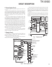
3-3. Driver and Final Power Amplifier Circuit
The transmit signal obtained from the TX VCO buffer am-
plifier Q311, is amplified to approximately +17dBm by the
driver amplifiers Q313, Q1 and Q2. This amplified signal is
passed to the power amplifier module (power module) IC1,
which consists of a MOS-FET amplifier and is capable of
transmission output power.
3-4. Automatic Power Control Circuit
The automatic transmission power control (APC) circuit
stabilizes the transmitter output power at a predetermined
level by detecting the power module output with a diodes
D6, D7 and D8. Diodes D6, D7 and D8 apply a voltage to DC
amplifier IC72 (A/2). IC72 (B/2) compares the APC control
voltage (PC) generated by microprocessor IC404 and DC am-
plifier IC71 (A/2, B/2) with the detection output voltage
from IC72 (A/2) to control the Vgg pin of IC1, and stabilizes
transmission output.
The APC circuit is configured to protect over-current of the
power module due to fluctuations of the load at the antenna
end and to stabilize transmission output at voltage and tem-
perature variations.
AMP
SW
SW
IC414Q416
Q417
AMP
DC
AMP
IC408
LPF
IC409
IC410 IC412IC415
D-SUB
MI2
AQUA-L
MOD
D-SUB
DI
DAC
MB
(for VCXO)
MOD
(for VCO)
MIC
J901
Mojular
jack
DISPLAY UNIT
(X54-348) TX-RX UNIT (X57-699)
IC413
Multi-
plexer
TXIN
LSDO
TX VCO
VCXO
16.8MHz
Q307
Q313
Drive
AMP
Q311
Buff
AMP
Q1
Drive
AMP
Q2
Drive
AMP
IC1
Final
AMP
X301
MOD
MB
DC
AMP
DC
AMP
PC
MP
SW
D2,D3,
D11
DET
DET
D6 D7
DET
D8
ANT
Gate
bias
IC71 IC72
CIRCUIT DESCRIPTION
Fig. 2 Microphone and modultion level adjustment circuit
Fig. 3 Drive and Final power amplifier and automatic power control circuit


