


NWZ-X1050/X1051/X1060/X1061
NWZ-X1050/X1051/X1060/X1061
2727
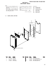
SECTION 4
DIAGRAMS
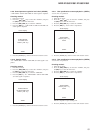
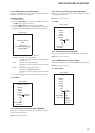
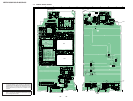
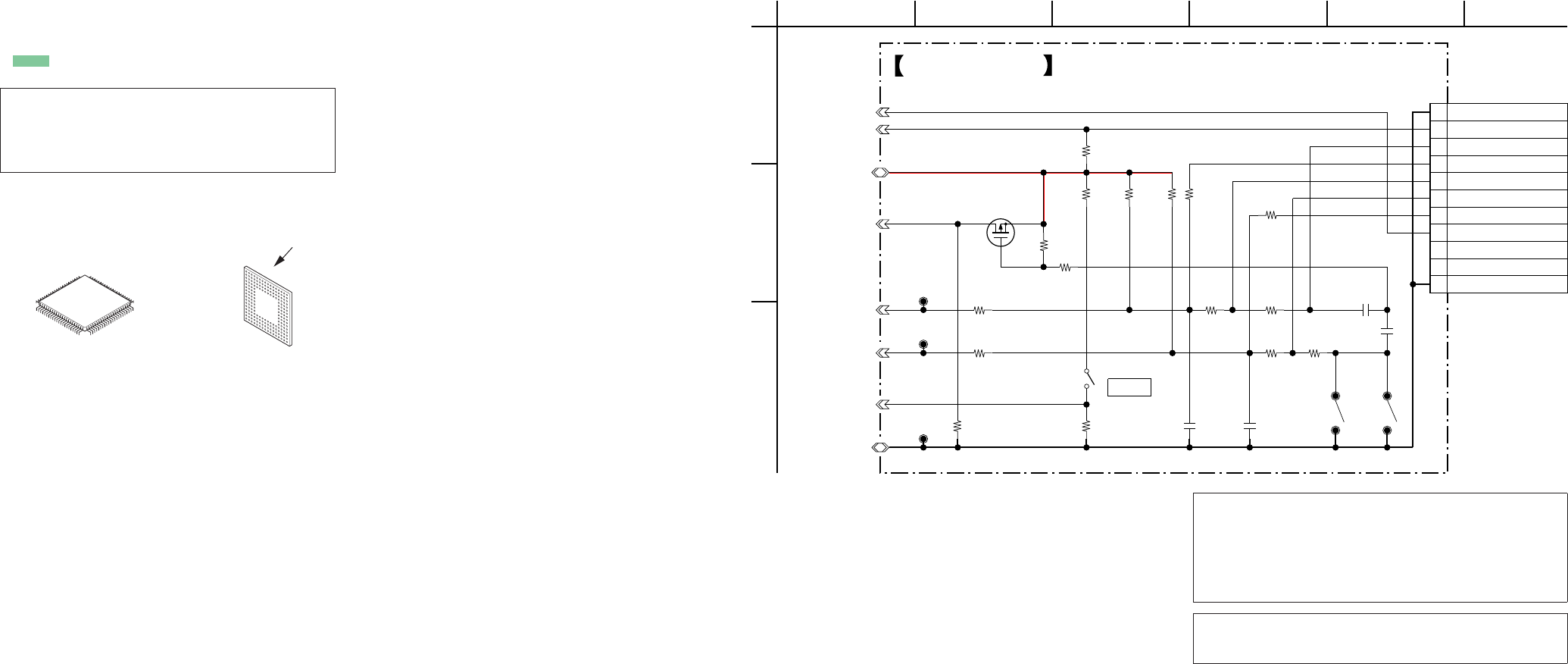
4-1. SCHEMATIC DIAGRAM
For Schematic Diagrams.
Note:
• All capacitors are in μF unless otherwise noted. (p: pF) 50
WV or less are not indicated except for electrolytics and
tantalums.
• All resistors are in Ω and 1/4 W or less unless otherwise
specifi ed.
• C : Panel designation.
• A : B+ Line.
THIS NOTE IS COMMON FOR PRINTED WIRING BOARDS AND SCHEMATIC DIAGRAMS.
(In addition to this, the necessary note is printed in each block.)
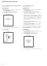
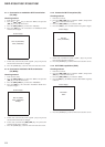
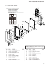
For Printed Wiring Boards.
Note:
• Y : Parts extracted from the conductor side.
• : Pattern from the side which enables seeing.
(The other layers' patterns are not indicated.)
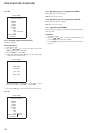
Caution:
Pattern face side:
(SIDE B)
Parts face side:
(SIDE A)
Parts on the pattern face side seen
from the pattern face are indicated.
Parts on the parts face side seen from
the parts face are indicated.
• MAIN board is muliti-layer printed board.
However, the patterns of intermediate-layers have not been in-
cluded in diagrams.
• Lead layouts
surface
CSP (Chip Size Package) Lead layout of conventional IC
Note 2: When the MAIN board is replaced, there are some notes.
Refer to “NOTE THE MAIN BOARD REPLACING” (page
4) in servicing notes for notes.
Note 1: In this set, only a part of parts that relate to the switch
are supplied. Therefore, the schematic diagram excerpts
and has described only a part. Replace a part according
to “METHOD OF JUDGING RIGHT AND WRONG OF
PARTS RELATED TO SWITCH” (page 7) in servicing
notes. Exchange the entire mounted board when parts that
do not correspond to it are defective.
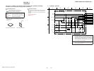
CL881
CL882
CL883
KEY_AD0
KEY_AD1
DGND
11P
CN881
1GND
2NC
3FR
4PLAY
5FF
6VOL+
7VOL-
8 RESET
9
10
11 GND
3LP01S-K-TL-E
Q881
VDD_GP1_J
KEY_WAKE
NC_ON
XHOLD_KEY
CL886
CL887
CL884
CL885
EXTRST
0.01
C884
0.01
C883
C881
0.047
C882
0.047
470k
R893
47k
R886
100
R895
47k
R887
470k
R883
R892
470k
10k
R889
470k
R881
10k
R890
10k
R891
0
R897
10k
R888
1k
R885
1k
R882
1k
R884
100
R896
S
HOLD
S881
MAIN BOARD
(KEY_AD0)
(KEY_AD1)
(GND)
4
B
635
C
1
A
2