


SP200/210 Maxon SP200/210 Radio
Issue 1.0 TABLE OF CONTENTS
03/01 Page v
Figure 6-1 – Legend Layout for Top Side of Digital PCB ...............................................................................6-5
Figure 6-2 - Legend Layout for Bottom Side of Digital PCB...........................................................................6-6
Figure 6-3 - Legend Layout for Top Side of RF PCB .....................................................................................6-7
Figure 6-4 - Legend Layout for Bottom Side of RF PCB ................................................................................6-8
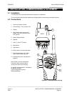
Figure 8-1 - Exploded Mechanical Drawing 1.................................................................................................8-3
Figure 8-2 - Exploded Mechanical Drawing 2.................................................................................................8-5
Figure 8-3 – Exploded Mechanical Drawing 3................................................................................................8-6
Figure 9-1 – Digital Board Layout Top Side....................................................................................................9-3
Figure 9-2 - Digital Board Layout Bottom Side ...............................................................................................9-4
Figure 9-3 - RF Board Layout Top Side..........................................................................................................9-5
Figure 9-4 - RF Board Layout Bottom Side ....................................................................................................9-6
Figure 9-5 – Front-End Board Layout.............................................................................................................9-7
Figure 9-6 – VCO Board Layout .....................................................................................................................9-7
Figure 9-7 – TCXO Board Layout...................................................................................................................9-8
Figure 11-1 – Calibration Program Initial Screen .........................................................................................11-1
Figure 11-2 - Calibration Program Primary Screen ......................................................................................11-2
Figure 11-3 - ASIC Control Screen (Rx).......................................................................................................11-3
Figure 11-4 - ASIC Control Screen (Tx) .......................................................................................................11-4
Figure 11-5 - ASIC Control Screen (Rx).......................................................................................................11-5
Figure 11-6 - Modulation wave shape ..........................................................................................................11-6
LIST OF TABLES
Table 6-1 – Diagnostics ..................................................................................................................................6-1
Table 6-2 – Troubleshooting chart..................................................................................................................6-2
Table 6-3 - Main Circuit Transistor Voltages ..................................................................................................6-3
Table 6-4 - Integrated Circuit Voltages (Receive) ..........................................................................................6-4
Table 6-5 - Integrated Circuit Voltages (Transmit) .........................................................................................6-4
Table 8-1 - Parts List for Exploded Mechanical Drawing 1.............................................................................8-4
Table 8-2 - Parts List for Exploded Mechanical Drawing 2.............................................................................8-6
Table 3 – V1 Default Frequency Table.........................................................................................................11-8
Table 4 – V1 Default ASIC Settings..............................................................................................................11-8
Table 5 – V2 Default Frequency Table.........................................................................................................11-9
Table 6 – V2 Default ASIC Settings..............................................................................................................11-9
Table 7 - U1 Default Frequency Table........................................................................................................11-10
Table 8 - U1 Default ASIC Settings ............................................................................................................11-10
Table 9 – U2 Default Frequency Table.......................................................................................................11-11
Table 10 – U2 Default ASIC Settings .........................................................................................................11-11