


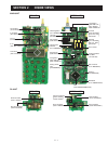
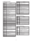

5 - 6
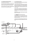
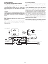
5-5-1 CPU (IC22)
Pin
No.
Port
Name
Description
1−3
KR1−
KR3
Input ports for dealer-programmable keys.
4−8
KS0−
KS4
Output ports for dealer-programmable keys.
9 BUSY Outputs “BUSY” signal to the DSP UNIT.
10 CCS Outputs chip-select signal to the DSP UNIT.
11 SCK
Outputs serial clock signal to the PLL IC (IC2, pin 9)
and D/A converter (IC12, pin 7/IC23, pin 7).
19−
21
CENC0−
CENC2
Output ports for CTCSS/DTCS signal.
22 S5C
Outputs S5V line control signal to the S5V
regurator (Q23).
“Low”=While power save mode.
26 T5C
Outputs T5V line control signal to the T5V line
regurator (Q24, Q49).
“Low”=While transmitting.
27 R5C
Outputs R5V line control signal to the R5V line
regurator (Q25).
“Low”=While receiving.
31 PLST Outputs PLL strobe signal to the PLL IC (IC2, pin 11).
34 ULCK
Input port for PLL unlock detect signal from the
PLL IC (IC2, pin 7).
“Low”=While the PLL circuit is unlocked.
35 TMUT
Outputs transmit mute signal to the transmit mute
switch (Q46).
“High”=Transmitting is muted.
36 MONI
Input port for [SIDE1] key (S5).
“Low”=While the key is pushed.
37 EMER
Input port for top switch (S1).
“Low”=While the switch is pushed.
39 DSDA Outputs serial data to the D/A converter (IC23, pin 6).
43 SENC Outputs DTMF signals to the LPF (IC6, pin 3).
44 BEEP
Outputs beep sounds to the D/A converter (IC12,
pin 21).
45 SDEC Input port for DTMF signals.
46 CDEC Input port for CTCSS/DTCS signals.
48 BATV Input port for remaining battery power.
49 LVIN Input port for VCO lock voltage.
50 RSSI
Input port for receive signal strength level signal
from the FM IF IC (IC9, pin 12).
59 RES
Input port for CPU reset signal from the reset IC
(IC8, pin 1).
“Low”=When the CPU is reset.
69 CSFT
Outputs CPU clock shift signal to the clock shift
switch (D6).
70 AFON
Outputs AF power amplifi er (IC15) control signal to
the AF power amplifi er controller (Q41, Q42, D21,
D23).
“High”=The AF power amplifi er is ON.
71 DAST
Outputs strobe signal to the D/A converter (IC12,
pin 6).
72 DUSE
Outputs CTCSS/DTCS select signal to the tone
fi lter switch (Q40).
“High”=While DTCS is in use.
75 NOIS
Input port for noise signal from the FM IF IC (IC9,
pin 13).
82 ESDA Outputs serial data to the EEPROM (IC10, pin 5).
85 ESCL Outputs clock signal to the EEPROM (IC10, pin 6).
Pin
No.
Port
Name
Description
89 DIGI
Outputs Analog/Digital select signal to the A/D
switch (D2, D3).
“High”=Digital mode is selected.
91 LSO Outputs serial data to the LCD driver (IC20, pin 48).
92 LSCK Outputs clock signal to the LCD driver (IC20, pin 47).
93 LCS
Outputs chip-enable signal to the LCD driver (IC20,
pin 46).
94 LINH
Outputs display inhibit signal to the LCD driver
(IC20, pin 45).
95 LIGT
Outputs LCD backlight control signal to the
backlight LED’s (DS1, DS2) driver (Q45).
“Low”=While the backlight is ON.
96 RMUTE
Outputs AF mute signal to the analog switch (IC3,
pins 12, 13).
“Low”=While the squelch is close or transmitting.
97 MMUTE
Outputs MIC signals mute signal to the analog
switch (IC3, pin 5) and MIC mute switch (Q31).
“Low”=While receiving.
99 SSO
Outputs serial data to the PLL IC (IC2, 10) and D/A
converter (IC12, pin 8).
100 KR0 Input ports for dealer-programmable keys.
5-5-2 D/A CONVERTER (IC12)
Pin
No.
Port
Name
Description
2MCGO
Outputs level-adjusted MIC signals to the MIC mute
switch (Q31).
10,
16
MOD
Outputs modulation signal to the modulation circuits
(D2).
14 REF
Outputs reference frequency control voltage to the
reference frequency oscillator buffer (IC7, pin 13).
15 BAL
Outputs modulation balance control signal to the
reference frequency oscillator buffer (IC7, pin 12).
22 BEEPO
Outputs beep sounds to the AF volume buffer (IC6,
pin 9).
23 SQLC
Outputs level-adjusted AF signals to the noise filter
(IC9, pins 7, 8,
R42, R44−R46, C69, C70, C413).
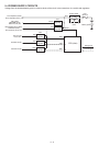
5-5-3 D/A CONVERTER (IC23)
Pin
No.
Port
Name
Description
1T1
• While receiving
Outputs BPF tuning voltage to the tunable BPF
(D19, D25, L7, L8, C21−C23, C25, C27−C29).
• While transmitting (as “APC” signal)
Outputs transmit mute signal to the transmit mute
switch (Q46).
2T2
Outputs BPF tuning voltage to the tunable BPF
(
D14, D15, L9, L11, C19, C36, C39−C41,
C44, C45
).
3TXLVA
Outputs oscillating frequency adjust voltage to the
TX VCO (Q16, D10, D13).
4RXLVA
Outputs oscillating frequency adjust voltage to the
RX VCO (
Q17, D9, D11).
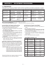
5-5 PORT ALLOCATIONS