


5 - 4
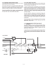
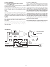
5-3 PLL CIRCUITS
5-3-1 VOLTAGE CONTROLLED OSCILLATORS
(VCOs; MAIN UNIT)
VCO is an oscillator whose oscillating frequency is controlled
by adding voltage (lock voltage).
This transceiver has 2 VCOs RX VCO (Q17, D9, D11, D33)
and TX VCO (Q16, D10, D13, D34). The RX VCO oscillates
the 1st LO signals, and the TX VCO oscillates the transmit
signal.
• RX VCO
The output signals are amplifi ed by the buffer amplifi ers (Q15,
Q29), and applied to the 1st mixer (Q6) via TX/RX switches
(D16 is OFF, D17 is ON) and LPF (L46, C396, C397), to be
mixed with the received signals to produce the 46.35 MHz 1st
IF signal.
• TX VCO
The output signal is applied to the transmit amplifi ers via the
buffer amplifi ers (Q15, Q29) and TX/RX switches (D16 is ON,
D17 is OFF).
A portion of each VCO output is applied to the PLL IC (IC2,
pin 8) via the buffer amplifi er (Q15), doubler (Q14), BPF (D31,
D32, L32, C196, C197, C199, C200, C205) and LPF (L34,
L36, C202–C204).
5-3-2 PLL IC (MAIN UNIT)
The PLL circuit provides stable oscillation of the transmit
frequency and receive 1st LO frequency. The PLL output
frequency is controlled by the divided ratio (N-data) from the
CPU.
The VCO output signal from the LPF (L34, L36, C202–C204) is
applied to the PLL IC (IC2, pin 8). The applied signal is divided
at the prescaler and programmable counter according to the
“SSO” signal from the CPU (IC22, pin 99). The divided signal
is phase-compared with the reference frequency signal from
the reference frequency oscillator (X2), at the phase detector.
The phase difference is output from pin 5 as a pulse type
signal after being passed through the internal charge pump.
The output signal is converted into the DC voltage (lock
voltage) by passing through the loop filter (R94–R96, C16,
C17, C146). The lock voltage is applied to the varactors (D9
and D33 of RX VCO, D10 and D34 of TX VCO) and locked to
keep the VCO frequency constant.
If the oscillated signal drifts, its phase changes from that of
the reference frequency, causing a lock voltage change to
compensate for the drift in the VCO oscillating frequency.
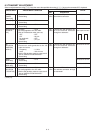
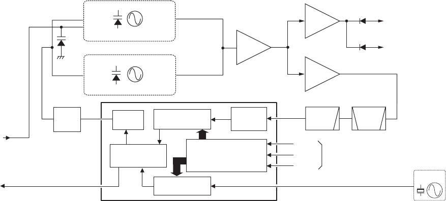
• PLL CIRCUITS
Loop
filter
Modulation signals
from the D/A converter
(IC12, pin10)
RX VCO
Q16, D10, D13, D34
D12
Q17, D9, D11, D33
TX VCO
PLL control signals from the CPU (IC22)
PLL unlock signal
to the CPU (IC22, pin 34)
15.3 MHz
reference frequency signal
Buffer
Buffer
×2
to the transmit amplifiers
to the1st IF circuits
D17
D16
BPF
PLST
SSO
SCK
5
7
8
1
9
10
11
PLL IC (IC2)
Shift register
Prescaler
Phase
detector
Charge
pump
Programmable
divider
Reference
counter
Q15
Q29
Q14
X2
TCXO
LPF