


4 - 3
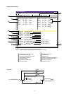
4-3 PLL CIRCUIT
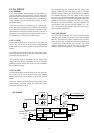
4-3-1 GENERAL
A PLL circuit provides stable oscillation of the transmit fre-
quency and receive 1st LO frequency. The PLL output com-
pares the phase of the divided VCO frequency to the refer-
ence frequency. The PLL output frequency is controlled by a
crystal oscillator and the divided ratio (N-data) of a pro-
grammable divider.
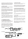
The PLL circuit, using a one chip PLL IC (IC1), directly gen-
erates the transmit frequency and divided ratio based on
serial data from the CPU and compares the phases of VCO
signals with the reference oscillator frequency. The PLL IC
detects the out-of-step phase and output from pin 5.The ref-
erence frequency (15.3 MHz) is oscillated by X1.
4-3-2 TX LOOP
The generated signal at the TX-VCO (Q11, D7) enters the
PLL IC (IC1, pin 8) and is divided at the programmable
divider section and is then applied to the phase detector
section.
The phase detector compares the input signal with a refer-
ence frequency, and then outputs the out-of-phase signal
(pulse-type signal) from pin 5.
The pulse-type signal is converted into DC voltage (lock
voltage) at the loop filter (R40–R42, C75–C77), and then
applied to varactor diodes (D6) of the TX-VCO to stabilize
the oscillated frequency.
4-3-3 RX LOOP
The generated signal at the RX-VCO (Q10, D5) enters the
PLL IC (IC1, pin 8) and is divided at the programmable
divider section and is then applied to the phase detector
section.
The phase detector compares the input signal with a refer-
ence frequency, and then outputs the out-of-phase signal
(pulse-type signal) from pin 5.
The pulse-type signal is converted into DC voltage (lock
voltage) at the loop filter (R40–R42, C74–C77), and then
applied to varactor diodes (D5) of the RX-VCO to stabilize
the oscillated frequency. The lock voltage is also used for
the receiver circuit for the bandpass filter center frequency.
The lock voltage from the loop filter is amplified at the buffer
amplifier (Q13) and then applied to the CPU (IC7, pin 60).
The signal is analyzed at the CPU, and then applied to the
D/A convertor (IC9). The D/A convertor outputs “T1”, “T2”,
“T3”, “T4” signals to RF bandpass filters D12–D15 to sup-
press harmonic components.
4-3-4 VCO CIRCUIT
The VCO outputs from Q11 (TX) and Q10 (RX) are buffer
amplified at Q7 and Q6, and are then sent to the T/R switch
(D3, D4). The receive LO signal is applied to the 1st mixer
circuit (Q19) through an attenuator, and the tramsmit signal
is applied to the YGR amplifier (Q4). A portion of the VCO
output is reapplied to the PLL IC (IC1, pin 8) via the buffer
amplifier (Q6) and low-pass filter (L18, R53, C89–C91).
Shift register
Prescaler
Phase
detector
Loop
filter
Programmable
counter
Programmable
divider
X1
15.2 MHz
45.9 MHz signal
to the FM IF IC
Q11, D7
TX VCO
RX VCO
Buffer
Buffer
Buffer
Q5
Q6
Q7
11
9
10
P.STB
IC1 (PLL IC)
CK
DATA
to transmitter circuit
to 1st mixer circuit
D3
D4
2
1
5
8
Q10, D5
Crystal
oscillator
×3
Q18
LPF
PLL CIRCUIT