


4 - 1
SECTION 4 CIRCUIT DESCRIPTION
4-1 RECEIVER CIRCUITS
4-1-1 ANTENNA SWITCHING CIRCUIT
The antenna switching circuit functions as a low-pass filter
while receiving. However, its impedance becomes very high
while D9 and D10 are turned ON. Thus transmit signals are
blocked from entering the receiver circuits. The antenna
switching circuit employs a
λ
⁄4 type diode switching system.
Received signals are passed through the low-pass filter (L1,
L2, C3, C5, C6). The filtered signals are applied to the
λ
⁄4
type antenna switching circuit (D9, D10).
The passed signals are then applied to the RF amplifier cir-
cuit.
4-1-2 RF CIRCUIT
The RF circuit amplifies signals within the range of frequen-
cy coverage and filters out-of-band signals.
The signals from the antenna switching circuit are amplified
at the RF amplifier (Q15) after passing through the tunable
bandpass filter (D12, L21, C104, C105). The amplified sig-
nals are applied to the 1st mixer circuit (Q19) after out-of-
band signals are suppressed at the 3 stages tunable band-
pass filter (D13, L22, C111, C113, D14, L23, C116, C117,
D15, L24, C120, C122).
Varactor diodes are employed at the bandpass filters that
track the filters and are controlled by the CPU (IC7) via the
D/A convertor (IC9) using T1–T4 signals. These diodes tune
the centre frequency of an RF passband for wide bandwidth
receiving and good image response rejection.
4-1-3 1ST MIXER AND 1ST IF CIRCUITS
The 1st mixer circuit converts the received signal into a fixed
frequency of the 1st IF signal with a PLL output frequency.
By changing the PLL frequency, only the desired frequency
will pass through a crystal filter at the next stage of the 1st
mixer.
The signals from the RF circuit are mixed at the 1st mixer
(Q16) with a 1st LO signal (393.65–423.65 MHz) coming
from the VCO circuit to produce a 46.35 MHz 1st IF signal.
The 1st IF signal is applied to a crystal filter (FI1) to sup-
press out-of-band signals. The filtered 1st IF signal is
applied to the IF amplifier (Q17), then applied to the 2nd
mixer circuit (IC3, pin 16).
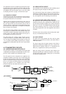
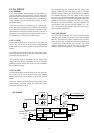
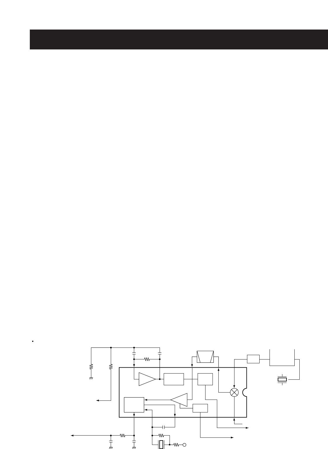
4-1-4 2ND IF AND DEMODULATOR CIRCUITS
The 2nd mixer circuit converts the 1st IF signal into a 2nd IF
signal. A double conversion superheterodyne system (which
converts receive signals twice) improves the image rejection
ratio and obtains stable receiver gain.
The 1st IF signal from the IF amplifier is applied to the 2nd
mixer section of the FM IF IC (IC3, pin 16), and is mixed with
the 2nd LO signal to be converted into a 450 kHz 2nd IF sig-
nal.
The FM IF IC contains the 2nd mixer, limiter amplifier, quad-
rature detector and active filter circuits. A 2nd LO signal
(45.9 MHz) is produced at the PLL circuit by tripling it’s ref-
erence frequency.
The 2nd IF signal from the 2nd mixer (IC3, pin 3) passes
through a ceramic filter (FI2) to remove unwanted hetero-
dyned frequencies. It is then amplified at the limiter amplifi-
er (IC3, pin 5) and applied to the quadrature detector (IC3,
pins 10, 11) to demodulate the 2nd IF signal into AF signals.
4-1-5 AF CIRCUIT
AF signals from the FM IF IC (IC3, pin 9) are applied to the
analog switch (IC6, pin 1) after being passed through the
high-pass filter (IC5B, pins 5, 7) via the “DET” signal. The
signals pass through the low-pass filter (IC5D, pins 13, 14),
and then applied to the analog switch (IC6, pins 9, 10) again.
The output signals from the analog swtich (IC6, pin 11) are
applied to the AF power amplifier (IC4, pin 4) after being
passed through the [VOL] control (SW-A/SW-B unit; R143)
via the “VOLIN” and “VOLOUT” signals.
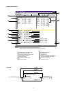
2ND IF AND DEMODULATOR CIRCUITS
Mixer
16
Limiter
amp.
2nd IF filter
450 kHz
PLL IC
IC1
X1
15.3 MHz
IC3 TA31136F
12
1st IF from the IF amplifier (Q17)
"RSSI" signal to the CPU pin 59
11109
87 5 3
AF signal "DET"
R5V
X2
R98
C155
C154
R100R99
R93
"SQLIN" signal to the
D/A convertor (IC9, pin 23)
R92
C138 C139
C140
2
21
Active
filter
FI2
Noise
detector
FM
detector
13
"NOIS" signal to the CPU pin 53
RSSI
Noise
comp.
×3
R94
Q18