


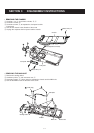
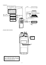

4 - 4
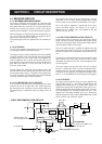
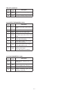
4-4 POWER SUPPLY CIRCUITS
VOLTAGE LINE
LINE
HV
VCC
CPU5V
T5V
R5V
S5V
+5V
VCO5V
DESCRIPTION
The voltage from the attached battery pack.
The same voltage as the HV line (battery volt-
age) which is controlled by the power swtich
([VOL] control).
Common 5 V converted from the VCC line by the
+5 regulator circuit (IC10). The output voltage is
applied to the CPU (IC7), reset circuit (IC8) and
etc.
5 V for transmitter circuits regulated by the T5
regulator circuit (Q27).
5 V for receiver circuits regulated by the R5 reg-
ulator circuit (Q26).
Common 5 V converted from the VCC line by the
S5 regulator circuit (Q24, Q19).
The same voltage as the CPU5V line for the ana-
log swtich (IC6), buffer amplifier (Q13), etc.
The same voltage as the +5V line for the TX-
VCO (Q11), RX-VCO (Q10) and buffer amplifiers
(Q5–Q7).
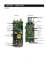
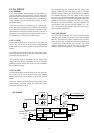
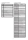
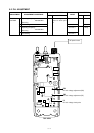
4-5 PORT ALLOCATIONS
4-5-1 CPU (IC7)
Pin
number
7
13
14
19
20
23
24
25
28
29
30
36
37
38
39
40
41
42
43
44
45
46
51
52
53
54
55
57
58
59
60
Port
name
RES
SENC0
SENC1
SENC2
SENC3
CENC0
CENC1
CENC2
SCK
SO
BEEP
PLST
DAST
EXST
PTT
TXC
RLED
TLED
AFON
ESDA
CLI
CLO
F1
F2
NOIS
UNLK
TEMP
CDEC
SDEC
RSSI
LVIN
Description
Input port for RESET signal.
Outputs single tone encode signal.
Outputs CTCSS/DTCS data signal.
Outputs serial clock signal to the PLL
IC (IC1), EEPROM (IC11), etc.
Outputs data signal to the PLL IC
(IC1) and D/A convertor (IC9).
Outputs beep audio signal.
I/O port for strobe signal from/to PLL
IC (IC9).
• Outputs strobe signal to the D/A con-
vertor (IC9).
• Input port for the initial version sig-
nal.
Outputs strobe signal for the expander
IC (IC15).
Input port for [PTT] swtich signal.
High: While [PTT] switch is pushed.
Outputs TX mute control signal.
High: While transmitting
Outputs BUSY LED control signal.
High: While receiving.
Outputs TX LED control signal.
high: While transmitting.
Outputs control signal for the regulator
circuit of AF power amplifier.
High: While squelch is open, etc.
I/O port for data signal from/to the
EEPROM (IC11).
Input port for cloning signal.
Outputs the cloning signal.
Input ports for the customization key
signals.
Input port for the noise pulse signal for
the squelch function.
Input port for PLL unlock signal.
High: PLL is locked.
Input port for the transceiver’s internal
tempereture detection.
Input port for CTCSS/DTCS signals.
Input port for single tone decode sig-
nal.
Input port for the RSSI voltage.
Input port for the PLL lock voltage.