


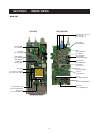
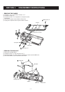

4 - 2
The applied AF signals are amplified at the AF power ampli-
fier circuit (IC4, pin 4) to obtain the specified audio level. The
amplified AF signals output from pin 10 as “AFOUT”signal
are applied to the internal speaker (SP1) as the “SP” signal
via the [SP] jack when no plug is connected to the jack.
4-1-6 SQUELCH CIRCUIT
A squelch circuit cuts out AF signals when no RF signals are
received. By detecting noise components in the AF signals,
the squelch switches the AF mute switch.
A portion of the AF signals from the FM IF IC (IC3, pin 9) as
“DET” signal are applied to the D/A convertor IC (IC9, pin
24). The signals from the D/A convertor (IC9, pin 23) as
“SQLIN” signals are applied to the active filter section (IC3,
pin 8) where noise components are amplified and detected
with an internal noise detector.
The active filter section amplifies noise components. The fil-
tered signals are rectified at the noise detector section and
converted into “NOIS” (pulse type) signals at the noise com-
parator section. The “NOIS” signal output from IC3, pin 13,
and is applied to the CPU (IC7, pin 53).
The CPU detects the receiving signal strength from the
number of the pulses, and outputs “EXST”, “SO”, “SCK” sig-
nals. The signals are applied to the expander IC (IC15, pins
1, 2, 3), and then outputs “RMUT” signal from pin 4. This sig-
nal controls the analog switch (IC6, pin 13) to cut the AF sig-
nal line.
4-2 TRANSMITTER CIRCUITS
4-2-1 MICROPHONE AMPLIFIER CIRCUIT
The microphone amplifier circuit amplifies audio signals with
+6 dB/octave pre-emphasis characteristics from the micro-
phone to a level needed for the modulation circuit.
The AF signals from the microphone are applied to the
microphone amplifier circuit (IC5c, pin 10) after being pass
through the high-pass filter (C186, C187). The amplified AF
signals are passed through the low-pass filter circuit (IC5d,
pins 13, 14) via the mute switch (IC6, pin 4). The filtered AF
signals are applied to the modulator circuit after being
passed through the mute switch (IC6, pins 8, 9, 10).
4-2-2 MODULATION CIRCUIT
The modulation circuit modulates the VCO oscillating signal
(RF signal) using the microphone audio signal.
The audio signals change the reactance of a diode (D6) to
modulate an oscillated signal at the TX-VCO circuit (Q11).
The oscillated signal is amplified at the buffer-amplifiers (Q5,
Q7), then applied to the T/R switching circuit (D3, D4).
4-2-3 DRIVE/POWER AMPLIFIER CIRCUITS
The signal from the VCO circuit passes through the T/R
switching circuit (D3) and is amplified at the YGR (Q4, Q3),
pre-drive (Q2) and power amplifier (Q1) to obtain 4 W of RF
power (at 7.2 V DC). The amplified signal passes through
the antenna switching circuit (D1) via the power detector
(D2), and low-pass filter and is then applied to the antenna
connector.
The bias current of the pre-drive (Q2) and the power ampli-
fier (Q1) is controlled by the APC circuit.
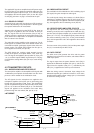
4-2-5 APC CIRCUIT
The APC circuit (IC2) protects the drive and the power
amplifiers from excessive current drive, and selects HIGH or
LOW output power.
The signal output from the power detector circuit (D2) is
applied to the differential amplifier (IC2, pin 3), and the “T4”
signal from the expander (IC9, pin 11), controlled by the
CPU (IC7), is applied to the other input for reference.
When the driving current is increased, input voltage of the
differential amplifier (pin 3) will be increased. In such cases,
the differential amplifier output voltage (pin 4) is decreased
to reduce the driving current.
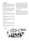
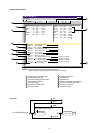
APC CIRCUIT
Q1
Power
amp.
Q2
Pre-driver
amp.
IC2
+
—
VCC
RF signal
from PLL
to antenna
T4
T5V
Q14
S5V
APC control circuit
Power detector
circuit (D2)
D2
LPF
D1
ANT
SW
AF
amp.
LPF
HPF
"DET" signal
from IC3, pin 9
"NWC" signal
from IC15, pin 14
Q21
Analog
switch
IC6
IC5B
IC5D
AF VOL.
R1
SW-A/SW-B
unit
IC4
SP
111
9, 102, 3
AF CIRCUIT