CIRCUIT DESCRIPTION
3-31
February 2001
Part No. 001-9800-001
oped across R606 and then fed to the power control
circuit. Reverse power is not detected in this
transceiver.
From the directional coupler the transmit signal is
fed to a low-pass harmonic filter formed by C624-
C627 and several sections of microstrip. This filter
attenuates harmonic frequencies occurring above the
transmit band. R607 dissipates static buildup on the
antenna.
The ambient power amplifier temperature is
sensed by thermistor R601. The resistance of a ther-
mistor decreases as temperature increases. This ther-
mistor forms a voltage divider with R143 on the audio/
logic board, and the voltage across this divider is
monitored by an A/D converter input of the microcon-
troller (pin 63). If the PA temperature increases above
limits set in software, the power is first cut back. Then
if it continues to rise, the transmitter is turned off.
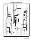
3.12.5 POWER CONTROL (U500A/B, Q500-
Q503)
Introduction
The power control circuit maintains a constant
power output as changes occur in temperature and
voltage. It does this by varying the supply voltage to
driver Q507. This changes the power output of that
stage which in turn controls the power output of the
transmitter.
The primary signal sensed to control power
output is forward power from the directional coupler.
The current to final amplifier Q601 is also sensed, but
it affects power output only if it becomes excessive.
Gradual power shutdown then occurs.
The power output level is set in 127 steps by the
microcontroller through D/A converter U801. This
allows power to be adjusted from the front panel using
the test mode and also different power levels to be
programmed for each system. In addition, it allows the
microcontroller to cut back power when power ampli-
fier temperature or transceiver voltage is excessive as
just described in Section 3.12.4.
U500A, Q500/Q502 Operation
U500A is a differential amplifier which ampli-
fies the difference between the reference voltage on
pin 3 and the forward power signal on pin 2. The
forward power signal from the directional coupler is a
DC signal that increases in proportion to forward
power. The reference input is a DC voltage from the
D/A converter formed by shift register U801 and
several resistors. This stage is similar to U305
described in Section 3.4.4, and programming of U801
is described in Section 3.10.9. This reference voltage
effectively sets the power output of the transmitter.
The turn-on time of U500A is controlled by the
time constant of C502 and R508. Negative AC feed-
back to prevent oscillation is also provided by C502.
This circuit operates as follows: Assume the output
power attempts to increase. The DC voltage applied to
U500A, pin 2 then increases which causes the output
voltage on pin 1 to decrease. Transistors Q502 and
Q500 then turn off slightly which decreases the supply
voltage to driver Q507. The output power then
decreases to maintain a constant power output. R510
and R513 limit the voltage gain of Q500 and Q503 to
approximately two.
Delayed PTT
Transistor Q503 is used to delay power output for
a short time after the transmitter is keyed. This allows
the synthesizer, Q506 in the exciter, and the first stage
of PA module U600 to stabilize so that the transmitter
does not transmit off-frequency. The signal which
controls Q503 is from the Q2 output (pin 17) of latch
U111 on the audio/logic board. In the receive mode,
this output is low which turns Q503 off. U500A, pin 2,
is then pulled high by 8 volts applied through R505
and CR503. The output of U500A on pin 1 is then low
which shuts off power to Q507. Then when the trans-
mitter is keyed, Q503 turns on after a short delay and
diode CR503 is no longer forward biased. Only the
forward power signal is then applied to pin 2 of
U500A.
800/900 MHz TRANSMITTER DESCRIPTION


