CIRCUIT DESCRIPTION
3-7
February 2001
Part No. 001-9800-001
NAND gates U104A and U104D provide gating
of the write signal to U108. Data is written to this
device only during Flash programming. Therefore,
when Flash programming occurs, the Q3 output (pin
16) of shift register U111 goes high which enables
U104A. A double inversion of the write signal then
occurs and it is applied to the WE
input of U108.
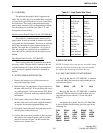
Latch Programming (U106, U110-U112)
Decoder U106 provides chip select to octal
latches U110, U111, and U112. When data is written
to U106 address space, a low signal is applied to chip
select input G2A
(pin 4) and a high signal is applied to
chip select input G1 (pin 6). The three address bits
applied to the A, B, and C inputs of U106 select one of
the eight outputs. When an output is selected, it goes
low.
Data is latched by U110-U112 on a rising edge of
a clock signal from U106. Therefore, when the U106
output is disabled, data is latched. The outputs of the
latches are enabled when the OC
input (pin 1) is low,
and the outputs are a high impedance state when it is
high.
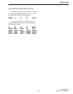
3.4 RECEIVE AUDIO/DATA PROCESSING
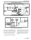
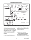
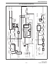
NOTE: A block diagram of the audio and data
processing circuitry is shown in Figure 3-3.
3.4.1 AMPLIFIER (U301B)
The demodulated receive audio/data signal from
limiter/detector U201 in the receiver is applied to
amplifier U301B. The gain of this amplifier is
controlled by analog switch U307B. The gain is higher
for narrow-band (12.5 kHz) channels to compensate
for the lower detected signal level that results from the
lower deviation used with those channels. The gain is
approximately four with narrowband channels and two
with wideband (25 kHz) channels.
The control input of U307B (pin 5) is low for
narrowband channels and high for wideband chan-
nels. When it is high, the switch is closed and R327 is
switched into the circuit. This adds more feedback
which decreases the gain. The control signal comes
from the Q0 output (pin 19) of latch U111. Transistor
Q305 inverts this signal and also provides level
translation from 5-volt logic levels of U111 to the 8-
volt logic levels of U307B.
From U301B the receive audio/data signal is fed
to audio, data, and squelch circuits. Refer to the
following descriptions for more information.
3.4.2 RECEIVE AUDIO PROCESSING
Bandpass Filter (U301C, U301D)
U301C and U301D form a bandpass filter which
passes frequencies in the 300-3000 Hz range. This
attenuates frequencies below 300 Hz such as LTR data
and Call Guard signaling, and frequencies above 3
kHz such as noise. These stages also provide 6 dB per
octave de-emphasis to remove the pre-emphasis that
was added to the signal when it was transmitted.
Mute Gate (U307C), Summing Amplifier (U301A)
The receive audio signal is then routed via the
option wireouts to mute gate U307C. This gate mutes
the signal when no carrier is being received or if the
message is intended for someone else. It is controlled
by the Q5 output (pin 14) of latch U110. When the
audio signal is muted, this output is high. This signal is
then inverted by Q301 resulting in a low signal on the
control input (pin 6) of gate U307C.
U301A is a summing amplifier which combines
the supervisory tone signal from microcontroller pin
36 (PA6) with the receive audio signal. Supervisory
tones include the busy and intercept tones and other
beeps that are heard by the user. C320 provides addi-
tional feedback of the higher frequencies present in the
square-wave output of the microcontroller. C323 and
R352 also provide shaping of this signal.
Audio Power Amplifier (U306)
The output signal from U301A is fed to the
microphone connector through C321 and to audio
power amplifier U306. This is a 5-watt (with an 8-ohm
load) bridge-type amplifier. Therefore, both outputs
are connected directly to the speaker and neither
speaker terminal is grounded. This device is internally
protected from damage resulting from shorting either
output to ground or B+, or shorting across the outputs.
AUDIO/LOGIC DESCRIPTION (ALL MODELS)


