CIRCUIT DESCRIPTION
3-14
February 2001
Part No. 001-9800-001
Part of the VCO output signal is fed out of the
VCO on pin 2 and applied to a second harmonic filter
formed by C842 and L802. A 50-ohm load is provided
by R855, with C841 providing impedance matching.
Part of the VCO signal is also fed out of the VCO
on pin 1 and applied to a 50-ohm, 3 dB pad formed by
R842, R839, and R843. The signal is then fed to buffer
amplifier Q801. Impedance matching is provided by
C822, C826, and L801, and temperature-compensated
bias is provided by R830, R833, R844, and CR801.
Transistor Q801 provides isolation and also amplifies
the signal to produce an output level of approximately
0 dBm. Capacitors C817 and C813 decouple RF
signals, and L800, C818, C827, R836, R837, and
R847 provide impedance matching and the proper
signal levels to the receiver and exciter. R832 lowers
the Q of L800 to make it less frequency selective.
3.7.4 VCO AND TCXO MODULATION
NOTE: If the wideband data input is used, the external
device must provide FCC-approved modulation limit-
ing and splatter filter circuitry and a stable 2.5 VDC
reference level.
Both the reference oscillator and VCO are modu-
lated in order to provide the required frequency
response. If only the VCO was modulated, the phase
detector in U804 would sense the frequency change
and change the control voltage to counteract the
change, especially at the lower audio frequencies. If
only the reference oscillator was modulated, the VCO
frequency would not change fast enough, especially at
the higher audio frequencies. By modulating both, a
relatively flat response is provided to all modulation
frequencies.
Separate audio, data, and wideband data modula-
tion signals are applied to the synthesizer on J201, pins
18, 17, and 16, respectively. The data signal includes
LTR and Call Guard signaling, while the wideband
data signal comes directly from an external device
such as a modem without passing through the limiting
and filtering circuitry.
The levels of the audio and data signals are set by
digitally controlled variable resistors in U802. These
resistors are adjusted in 256 steps by serial data from
the microcontroller (see Section 3.3.1). The transmit
audio signal is applied to pins 2 and 4 which are the
wiper and one leg of a potentiometer. It is fed out on
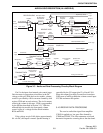
pin 3 which is the other leg of the potentiometer (see
Figure 3-4). Likewise, the data signal is fed in on pins
22 and 24 and out on pin 23.
These variable resistors set the modulation level
of the audio and data signals and also allow the micro-
controller to provide frequency compensation. This
compensation is required because modulation tends to
increase as the VCO frequency increases (tank circuit
capacitance decreases).
The output signals on pins 23 and 3 of U802 are
then combined with the wideband data signal and
applied to summing amplifier U803. The output signal
from U803 is then applied to the reference oscillator
on pin 1 and also to a potentiometer on pin 19 of
U802. The output on pin 18 of U802 is applied to the
VCO on pin 5. This modulates both the reference
oscillator and VCO, and the potentiometer in U802
adjusts the balance of these signals.
3.7.5 SYNTHESIZER INTEGRATED CIRCUIT
(U804)
Introduction
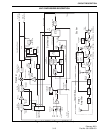
A block diagram of synthesizer IC U804 is shown
in Figure 3-5. This integrated circuit contains the
following stages. The basic operation of U804 is
described in Section 3.7.1.
• Reference divider
• Main divider
• Prescaler (÷64/65)
• Phase and lock detectors
• Charge pump and divider programming circuitry.
Channel Programming
Channels are selected by programming the main
divider in U804 to divide by a certain number. This
programming is performed by the microcontroller over
the SPI serial data bus which consists of CLOCK,
DATA, and STROBE lines (see Section 3.3.1). As
previously described, this divider is programmed so
that when the VCO is oscillating on the correct
frequency, the fR and fV inputs to the phase detector
are the same frequency.
UHF SYNTHESIZER DESCRIPTION


