


CIRCUIT DESCRIPTION
3-24
February 2001
Part No. 001-9800-001
VCO to the center of the operating band when the
control voltage is at its midpoint.
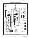
The output signal on the collector of Q902 is
coupled by C911 to a buffer amplifier formed by Q901
and Q903. This is a shared-bias amplifier which
provides amplification and also isolation between the
VCO and stages which follow. C918 provides imped-
ance matching on the input, and the resistors in the
circuit provide biasing and stabilization (R913 also
provides current limiting). C901, C902, and C908 are
RF decoupling capacitors, and C909 and C919 provide
an AC ground on the emitters of Q901 and Q903.
The output signal on the collector of Q903 is fed
through C914 to synthesizer U804. A 50-ohm load is
provided by R855, and C841, C842, and C849 provide
impedance matching. Likewise, the output signal on
the collector of Q901 is fed through C904 to buffer
amplifier Q801 (see Section 3.10.5). Resistor R902
lowers the Q of L903 to make is less frequency
selective.
VCO Frequency Shifting
In the applicable 800 or 900 MHz band, the VCO
must be capable of producing frequencies from the
lowest receiver first injection frequency up to the
highest talk-around mode transmit frequency. At 800
MHz, the lowest VCO frequency is 798.0625 MHz
(52.950 MHz below the lowest receive frequency of
851.0125 MHz) and the highest talk-around frequency
is 869.9875 MHz. Therefore, the VCO frequency band
spread is approximately 72 MHz. If this large
frequency shift was achieved only by varying the VCO
control voltage, the VCO gain would be undesirably
high. Instead, capacitance is switched in and out of the
tank circuit to provide a coarse frequency shift.
This switching is provided by PIN diode CR901
which is controlled by the logic signals from the Q0
and Q1 outputs (pins 4 and 5) of shift register U800.
Q803 and Q804 function as inverters and drivers.
When a PIN diode is forward biased, it presents a very
low impedance to RF signals. Conversely, when it is
reverse biased, it presents a very high impedance.
Forward biasing of PIN diode CR901 adds capac-
itance to the tank circuit which lowers its resonant
frequency. The diode is forward biased in the normal
mode and reverse biased in the talk-around mode (both
800 and 900 MHz). The logic levels on pins 3 and 4 of
the VCO are as follows:
Pin 3 Pin 4
Normal Mode H (5.5V) L (0V)
Talk-Around Mode L (0V) H (5.5V)
In the normal mode, CR901 is forward biased by
current flowing through R903, L905, CR901, and
L902. Capacitors C907 and C912 are then effectively
AC grounded through CR901 and C905. The control
lines are isolated from tank circuit RF by L902/C903,
L905/C906, C811, C812, C823, and C824.
Frequency Control and Modulation
Fine VCO frequency control is performed by
varying the DC voltage across varactor diodes CR903
and CR904 (coarse control is provided as described in
the preceding description). As the DC voltage applied
across a reverse-biased varactor diode increases, its
capacitance decreases. Therefore, the VCO frequency
increases as the control voltage increases and vice
versa. The amount of frequency change produced by
CR903 and CR904 is set by series capacitor C922. A
DC ground is provided by L908, and the control line is
isolated from tank circuit RF by L909 and C925.
The VCO is frequency modulated in a similar
manner. Another capacitance leg of the tank circuit is
formed by C915, C920, and varactor diode CR902.
The audio and data modulation signal is applied across
CR902, and a fixed bias from a voltage divider formed
by R853 and R854 is applied through R851 to pin 5.
Isolation and filtering of this DC bias is provided by
C838, C839, C840, and R852. Refer to the next
section for more information on modulation.
3.10.3 VCO AND TCXO MODULATION
NOTE: If the wideband data input is used, the external
device must provide FCC-approved modulation
limiting and splatter filter circuitry and a stable 2.5
VDC reference level.
Both the reference oscillator and VCO are modu-
lated in order to provide the required frequency
response. If only the VCO was modulated, the phase
detector in U804 would sense the frequency difference
and change the control voltage to counteract it, espe-
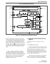
800/900 MHz SYNTHESIZER DESCRIPTION