TK-2160
8
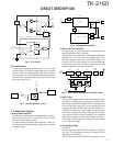
RECEIVE SIGNALING
RECEIVE SIGNALING
SP
Q608
SW
IF Amp
FM IF IC401
IC602
IF Amp
IC601
IC605
AF PA
IC805
IC603
BPF & COMPALATER
Q603,604,607
SW
QT/DQT
2-TONE
DTMF
CLK,DATA,
STD,LOADN
SIGNAL
SP MUTE
HSDI
LSDI
AN SQL
CPU
AQUA
CIRCUIT DESCRIPTION
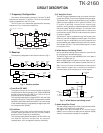
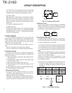
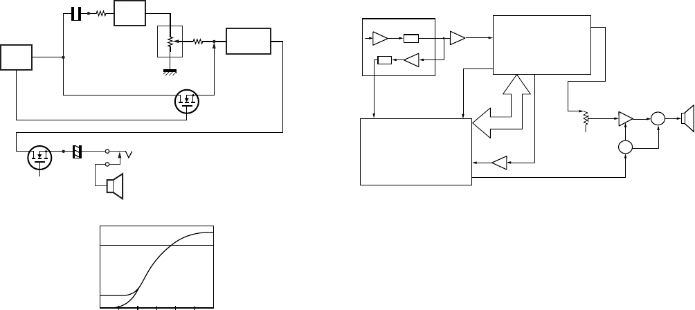
Fig. 5 AF amplifier and squelch
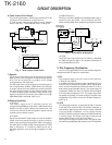
6) Tone Volume Fixed Circuit
This function generates a TONE signal sound even if the
AF volume of the transceiver is the minimum.
A TONE signal is sent through Q602 to the AF amplifier
when, in the FPU, “TONE Volume Fixed” is set to ON.
7) Squelch
Part of the AF signal from the IC enters the FM IC (IC401)
again, and the noise component is amplified and rectified
by a filter and an amplifier to produce a DC voltage
corresponding to the noise level.
The DC signal from the FM IC goes to the analog port of
the microprocessor (IC805). IC805 determines whether
to output sounds from the speaker by checking whether
the input voltage is higher or lower than the preset value.
To output sounds from the speaker, IC805 sends a high
signal to the SP MUTE line and turns IC605 on through
Q603,Q604,Q607 and Q608. (See Fig. 5)
8) Receive Signalling
(1) QT/DQT
The output signal from IF IC(IC401) enters the
microprocessor(IC805) through IC601. IC805 determines
whether the QT or DQT matches the preset value, and
controls the SP MUTE and the speaker output sounds
according to the squelch results.
(2) 2-TONE
Part of the received AF signal output from the AF amplifier
IC602, and then passes through an audio processor
(IC601), goes to the other AF amplifier IC603, is compared,
and then goes to IC805. IC805 checks whether 2-TONE
data is necessary. If it matches, IC805 carries out a
specified operation, such as turning the speaker on. (See
Fig. 5)
(4) DTMF
The DTMF input signal from the IF IC (IC401) is amplified
by IC602 and goes to IC601. The decoded information is
then processed by the CPU.
3. PLL Frequency Synthesizer
The PLL circuit generates the first local oscillator signal for
reception and the RF signal for transmission.
1) PLL
The frequency step of the PLL circuit is K:2.5,5,6.25 or
7.5kHz, M:6 or 6.25kHz.
A 16.8MHz reference oscillator signal is divided at IC1 by a
fixed counter to produce an oscillator (VCO) output signal
which is buffer amplified by Q9 then divided in IC1 by a
dual-module programmable counter. The divided signal is
compared in phase with the 5 or 6.25kHz reference signal
from the phase comparator in IC1. The output signal from
the phase comparator is filtered through a low-pass filter
and passed to the VCO to control the oscillator frequency.
(See Fig. 6)
2) VCO
The operating frequency is generated by Q6 in transmit
mode and Q5 in receive mode. The oscillator frequency is
controlled by applying the VCO control voltage, obtained
from the phase comparator, to the varactor diodes
(D3,D5,D7 and D8 in transmit mode and D4,D6,D9 and D10
in receive mode). The RX pin is set high in receive mode
causing Q8 and Q12 to turn Q6 off and Q5 on.
The TX pin is set high in transmit mode. The outputs from
Q5 and Q6 are amplified by Q9 and sent to the RF amplifiers.
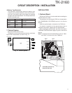
Fig. 4 Tone volume fixed circuit
IC805
CPU
BEEP
BEEPSW
TONE VOL FIXED
IC601
AQUA
VOL
IC605
TA7368F
Q602
Hi: ON
LOW: OFF
+
SP
SP-J
[VOL Position vs Output Level]
Output Level (mV)
Min
ON
OFF
25
500
Center Max
(3) MSK (Fleet Sync)
Fleet Sync utilizes 1200bps and 2400bps MSK signal is
output from pin 6 of IC601. And is routed to the VCO.
When encoding MSK, the microphone input signal is muted.


