CIRCUIT DESCRIPTION
3-12
February 2001
Part No. 001-9800-001
set the VCO to the center of the operating band when
the control voltage is at its midpoint.
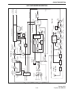
The output signal on the collector of Q102 is
coupled by C108 to a cascode buffer amplifier formed
by Q100 and Q101. This is a shared-bias amplifier
which provides amplification and also isolation
between the VCO and stages which follow. C113
provides impedance matching on the input, and the
resistors in the circuit provide biasing and stabilization
(R100 also provides current limiting). C100, C101,
and C106 are RF decoupling capacitors, and C105
provides an AC ground on the base of Q100.
The output signal on the collector of Q101 is
directly coupled to the emitter of Q100. Impedance
matching on the output of Q100 is provided by L100,
C102, and C103. Resistor R102 lowers the Q of L100
to make is less frequency selective. The VCO signal is
then fed to buffer Q801 and synthesizer chip U804 on
the RF board.
VCO Frequency Shifting
In a particular UHF band, the VCO must be
capable of producing frequencies from the receiver
first injection frequency for the lowest channel up to
the transmit frequency for the highest channel. Since
the first injection frequency is 45 MHz below the
receive frequency and the frequency band could be up
to approximately 42 MHz wide, this results in a
required VCO frequency spread of up to 87 MHz. If
this large frequency shift was achieved only by
varying the VCO control voltage, the VCO gain would
be undesirably high. Instead, capacitance is switched
in and out of the tank circuit to provide a coarse shift
in frequency and fine shift is provided by the control
voltage.
This switching is provided by PIN diodes CR104
and CR105 and controlled by a logic signal from the
Q0 and Q1 outputs (pins 4 and 5) of shift register
U800. When a PIN diode is forward biased, it presents
a very low impedance to RF signals. Conversely, when
it is reverse biased, it presents a very high impedance
to RF signals.
Forward biasing one of these PIN diodes adds
capacitance to the tank circuit which lowers its reso-
nant frequency. Capacitance is added to the circuit
when the control signal is low. Therefore, the lowest
frequency is selected when both control lines are low,
and the highest frequency is selected when both are
high.
For example, when Shift 1 goes low, CR104 is
forward biased by current flowing through R103 and
L105. Capacitor C111, which is part of the tank
circuit, is then effectively AC grounded through
CR104 and C107/C123. The control line is isolated
from tank circuit RF by choke L105 and decoupling
capacitor C104. The Shift 1 and Shift 2 logic signals
for each band segment are listed in Section 4.3.3.
Frequency Control and Modulation
Fine VCO frequency control is performed by
varying the DC voltage across varactor diodes CR103
and CR106 (coarse control is provided as described in
the preceding description). As the DC voltage applied
to a reverse-biased varactor diode increases, its capaci-
tance decreases. Therefore, the VCO frequency
increases as the control voltage increases and vice
versa. The amount of frequency change produced by
CR103 is set by series capacitor C118 and varactor
diode CR106. The control line is isolated from tank
circuit RF by L103 and C122.
The VCO is frequency modulated in a similar
manner. Another capacitance leg of the tank circuit is
formed by C116 and CR101. The audio and data
modulation signal is applied across varactor diode
CR101, and a fixed bias from a voltage divider formed
by R853 and R854 is applied through R851 to pin 5.
Isolation and filtering of this DC supply is provided by
C838, C839, C840, and R852. Refer to Section 3.7.4
for more information on modulation.
3.7.3 ACTIVE FILTER (Q800), BUFFER
AMPLIFIER (Q801)
Q800 functions as a capacitance multiplier to
provide a filtered 5.5-volt supply to the VCO. Resistor
R827 provides bias, and C814 provides the capaci-
tance that is multiplied. CR800 decreases the time
required to charge C814 when power is turned on. If a
noise pulse or other voltage change appears on the
collector, the base voltage does not change signifi-
cantly because of C814. Therefore, base current does
not change and the voltage on the emitter remains
constant.
UHF SYNTHESIZER DESCRIPTION


