


C8051F340/1/2/3/4/5/6/7
58 Rev. 0.5
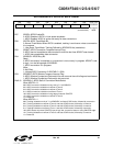
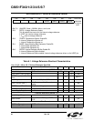
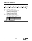
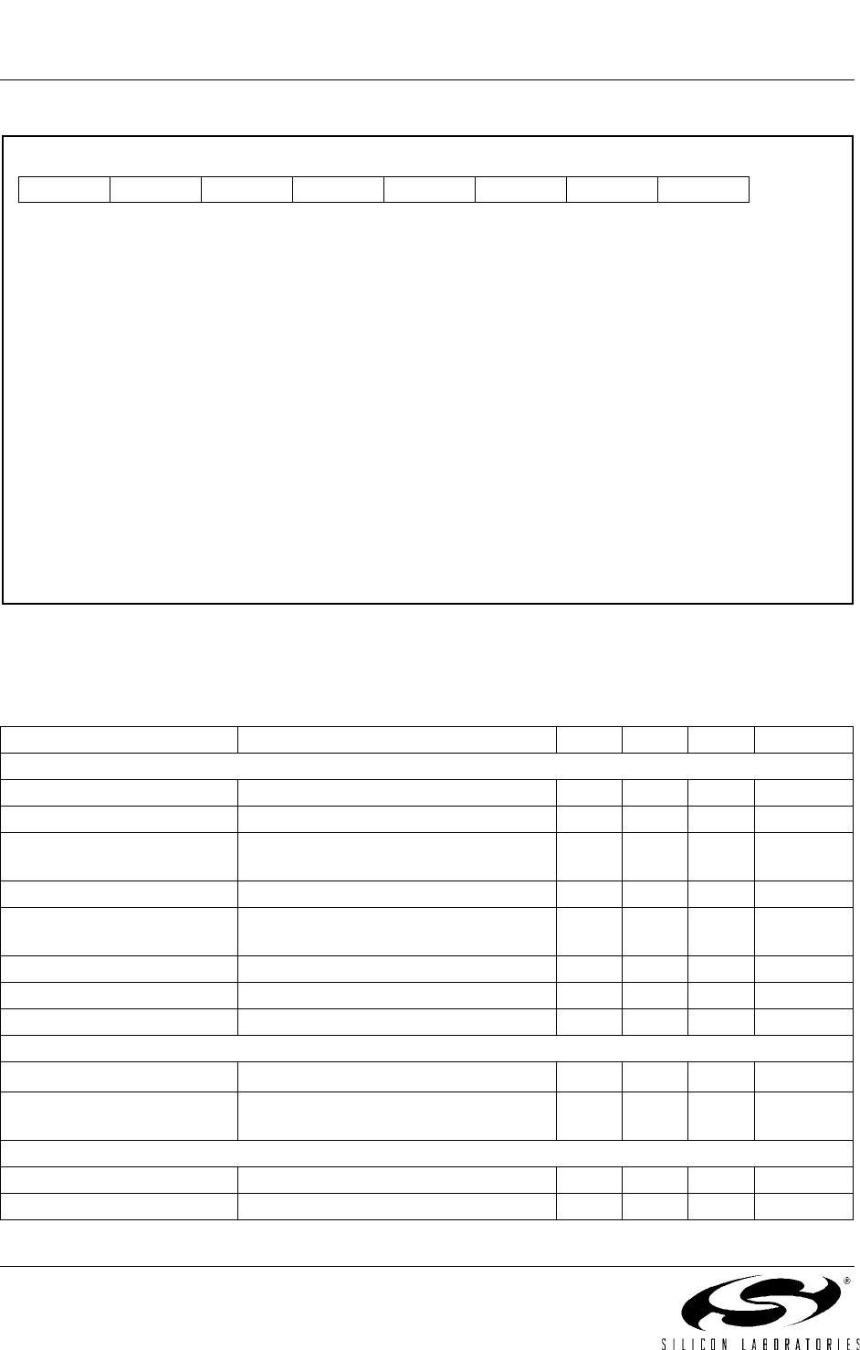
SFR Definition 6.1. REF0CN: Reference Control
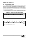
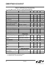
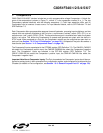
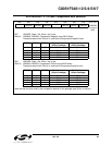
Table 6.1. Voltage Reference Electrical Characteristics
V
DD
= 3.0 V; –40 to +85 °C Unless Otherwise Specified
Parameter Conditions Min Typ Max Units
Internal Reference (REFBE = 1)
Output Voltage 25 °C ambient 2.38 2.44 2.50 V
VREF Short-Circuit Current 10 mA
VREF Temperature Coeffi-
cient
15 ppm/°C
Load Regulation Load = 0 to 200 µA to GND 1.5 ppm/µA
VREF Turn-on Time 1
4.7 µF tantalum, 0.1 µF ceramic
bypass
2 ms
VREF Turn-on Time 2 0.1 µF ceramic bypass 20 µs
VREF Turn-on Time 3 no bypass cap 10 µs
Power Supply Rejection 140 ppm/V
External Reference (REFBE = 0)
Input Voltage Range 0
V
DD
V
Input Current
Sample Rate = 200 ksps; VREF =
3.0
V
12 µA
Bias Generators
ADC Bias Generator BIASE = ‘1’ 100 µA
Reference Bias Generator 40 µA
Bits7–3: UNUSED. Read = 00000b; Write = don’t care.
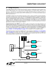
Bit3: REFSL: Voltage Reference Select.
This bit selects the source for the internal voltage reference.
0: VREF pin used as voltage reference.
1: V
DD
used as voltage reference.
Bit2: TEMPE: Temperature Sensor Enable Bit.
0: Internal Temperature Sensor off.
1: Internal Temperature Sensor on.
Bit1: BIASE: Internal Analog Bias Generator Enable Bit.
0: Internal Bias Generator off.
1: Internal Bias Generator on.
Bit0: REFBE: Internal Reference Buffer Enable Bit.
0: Internal Reference Buffer disabled.
1: Internal Reference Buffer enabled. Internal voltage reference driven on the VREF pin.
R/W R/W R/W R/W R/W R/W R/W R/W Reset Value
- - - - REFSL TEMPE BIASE REFBE 00000000
Bit7 Bit6 Bit5 Bit4 Bit3 Bit2 Bit1 Bit0 SFR Address:
0xD1