


Rev. 0.5 165
C8051F340/1/2/3/4/5/6/7
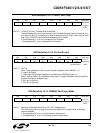
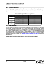
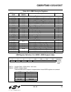
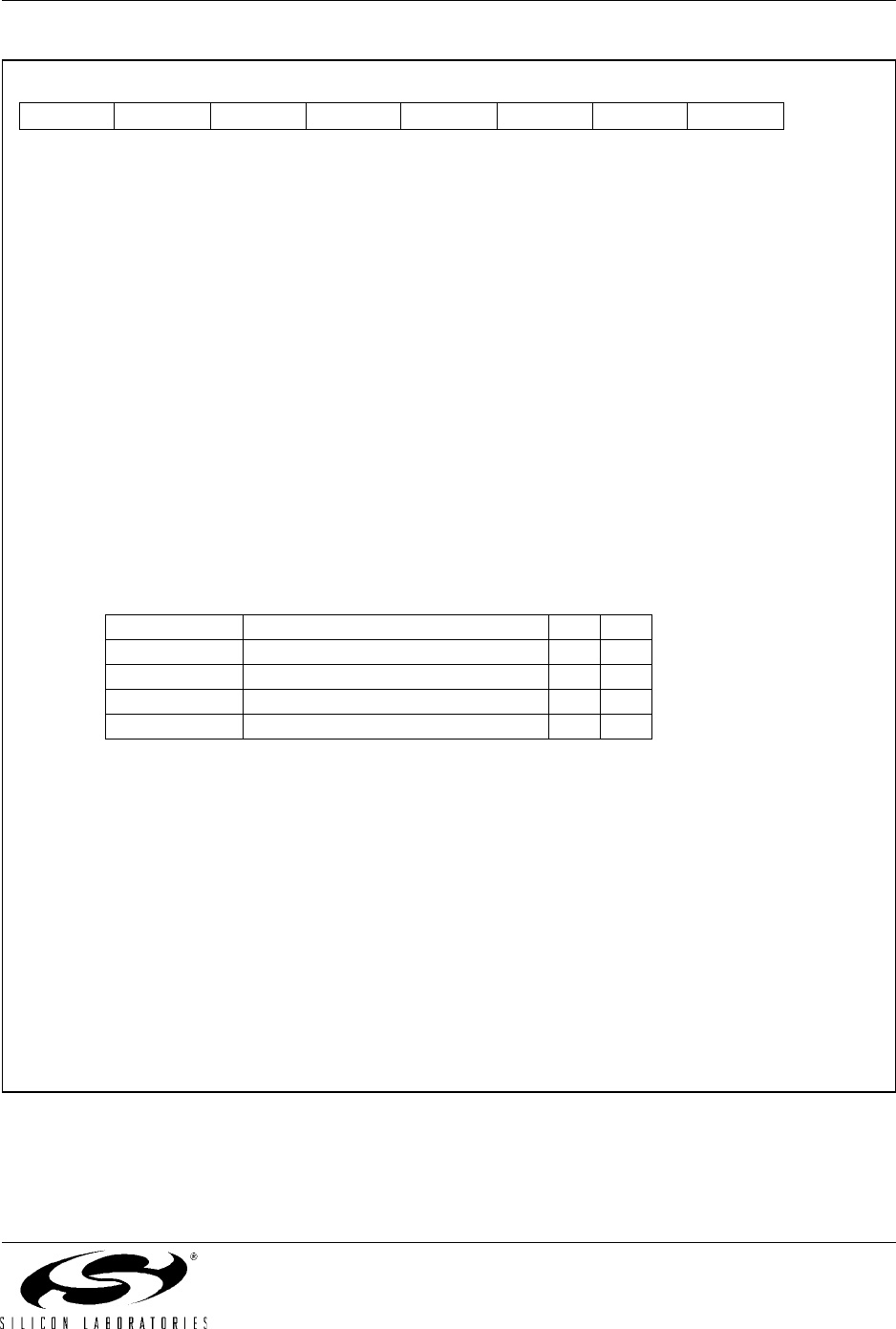
SFR Definition 16.1. USB0XCN: USB0 Transceiver Control
Bit7: PREN: Internal Pull-up Resistor Enable
The location of the pull-up resistor (D+ or D–) is determined by the SPEED bit.
0: Internal pull-up resistor disabled (device effectively detached from the USB network).
1: Internal pull-up resistor enabled when VBUS is present (device attached to the USB net-
work).
Bit6: PHYEN: Physical Layer Enable
This bit enables/disables the USB0 physical layer transceiver.
0: Transceiver disabled (suspend).
1: Transceiver enabled (normal).
Bit5: SPEED: USB0 Speed Select
This bit selects the USB0 speed.
0: USB0 operates as a Low Speed device. If enabled, the internal pull-up resistor appears
on the D– line.
1: USB0 operates as a Full Speed device. If enabled, the internal pull-up resistor appears on
the D+ line.
Bits4–3: PHYTST1–0: Physical Layer Test
These bits can be used to test the USB0 transceiver.
Bit2: DFREC: Differential Receiver
The state of this bit indicates the current differential value present on the D+ and D– lines
when PHYEN = ‘1’.
0: Differential ‘0’ signaling on the bus.
1: Differential ‘1’ signaling on the bus.
Bit1: Dp: D+ Signal Status
This bit indicates the current logic level of the D+ pin.
0: D+ signal currently at logic 0.
1: D+ signal currently at logic 1.
Bit0: Dn: D- Signal Status
This bit indicates the current logic level of the D– pin.
0: D– signal currently at logic 0.
1: D– signal currently at logic 1.
R/W R/W R/W R/W R/W R R R Reset Value
PREN PHYEN SPEED PHYTST1 PHYTST0 DFREC Dp Dn 00000000
Bit7 Bit6 Bit5 Bit4 Bit3 Bit2 Bit1 Bit0 SFR Address:
0xD7
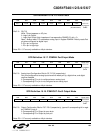
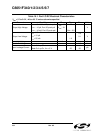
PHYTST[1:0] Mode D+ D–
00b Mode 0: Normal (non-test mode) X X
01b Mode 1: Differential ‘1’ Forced 1 0
10b Mode 2: Differential ‘0’ Forced 0 1
11b Mode 3: Single-Ended ‘0’ Forced 0 0