


C8051F340/1/2/3/4/5/6/7
104 Rev. 0.5
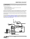
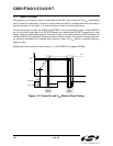
11.3. External Reset
The external /RST pin provides a means for external circuitry to force the device into a reset state. Assert-
ing an active-low signal on the /RST pin generates a reset; an external pull-up and/or decoupling of the /
RST pin may be necessary to avoid erroneous noise-induced resets. See
Table 11.1 for complete /RST pin
specifications. The PINRSF flag (RSTSRC.0) is set on exit from an external reset.
11.4. Missing Clock Detector Reset
The Missing Clock Detector (MCD) is a one-shot circuit that is triggered by the system clock. If more than
100
µs pass between rising edges on the system clock, the one-shot will time out and generate a reset.
After a MCD reset, the MCDRSF flag (RSTSRC.2) will read ‘1’, signifying the MCD as the reset source;
otherwise, this bit reads ‘0’. Writing a ‘1’ to the MCDRSF bit enables the Missing Clock Detector; writing a
‘0’ disables it. The state of the /RST pin is unaffected by this reset.
11.5. Comparator0 Reset
Comparator0 can be configured as a reset source by writing a ‘1’ to the C0RSEF flag (RSTSRC.5).
Comparator0 should be enabled and allowed to settle prior to writing to C0RSEF to prevent any turn-on
chatter on the output from generating an unwanted reset. The Comparator0 reset is active-low: if the
non-inverting input voltage (on CP0+) is less than the inverting input voltage (on CP0-), a system reset is
generated. After a Comparator0 reset, the C0RSEF flag (RSTSRC.5) will read ‘1’ signifying Comparator0
as the reset source; otherwise, this bit reads ‘0’. The state of the /RST pin is unaffected by this reset.
11.6. PCA Watchdog Timer Reset
The programmable Watchdog Timer (WDT) function of the Programmable Counter Array (PCA) can be
used to prevent software from running out of control during a system malfunction. The PCA WDT function
can be enabled or disabled by software as described in
Section “22.3. Watchdog Timer Mode” on
page 272; the WDT is enabled and clocked by SYSCLK / 12 following any reset. If a system malfunction
prevents user software from updating the WDT, a reset is generated and the WDTRSF bit (RSTSRC.5) is
set to ‘1’. The state of the /RST pin is unaffected by this reset.
11.7. Flash Error Reset
If a Flash read/write/erase or program read targets an illegal address, a system reset is generated. This
may occur due to any of the following:
• A Flash write or erase is attempted above user code space. This occurs when PSWE is set to ‘1’ and a
MOVX write operation is attempted above address 0x3DFF.
• A Flash read is attempted above user code space. This occurs when a MOVC operation is attempted
above address 0x3DFF.
• A Program read is attempted above user code space. This occurs when user code attempts to branch
to an address above 0x3DFF.
• A Flash read, write or erase attempt is restricted due to a Flash security setting (see Section
“12.3. Security Options” on page 111).
• A Flash Write or Erase is attempted when the V
DD
monitor is not enabled.
The FERROR bit (RSTSRC.6) is set following a Flash error reset. The state of the /RST pin is unaffected
by this reset.