


Rev. 0.5 23
C8051F340/1/2/3/4/5/6/7
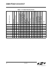
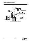
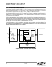
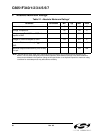
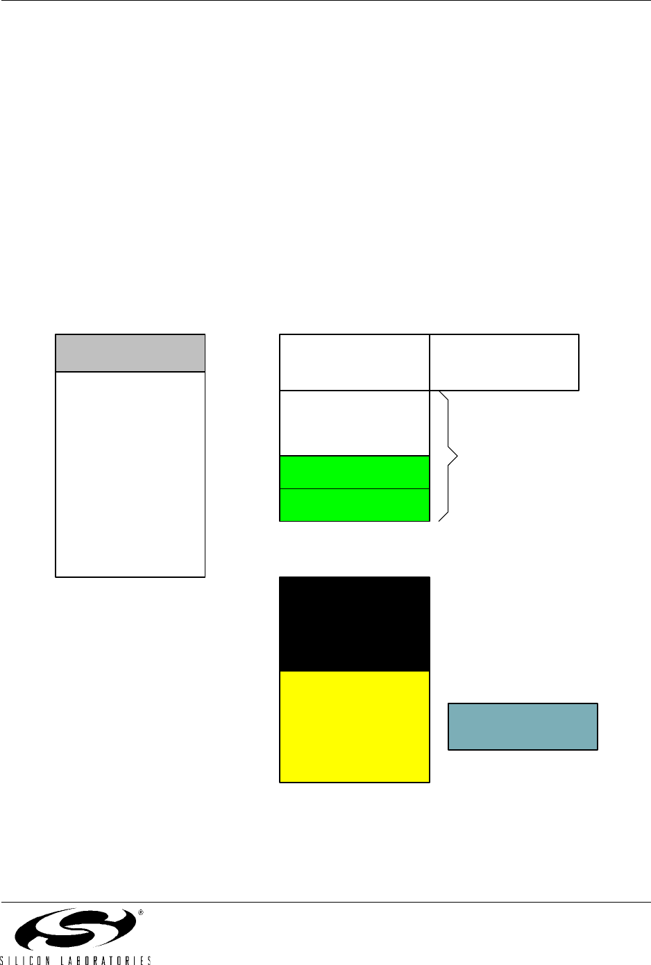
1.2. On-Chip Memory
The CIP-51 has a standard 8051 program and data address configuration. It includes 256 bytes of data
RAM, with the upper 128 bytes dual-mapped. Indirect addressing accesses the upper 128 bytes of general
purpose RAM, and direct addressing accesses the 128 byte SFR address space. The lower 128 bytes of
RAM are accessible via direct and indirect addressing. The first 32 bytes are addressable as four banks of
general purpose registers, and the next 16 bytes can be byte addressable or bit addressable.
Program memory consists of 64 k (C8051F340/2/4/6) or 32 k (C8051F341/3/5/7) bytes of Flash. This
memory may be reprogrammed in-system in 512 byte sectors, and requires no special off-chip program
-
ming voltage. On-chip XRAM is also included for the entire device family. The 64 k FLASH devices
(C8051F340/2/4/6) have 4
k of XRAM space. The 32 k Flash devices (C8051F341/3/5/7) have 2 k of
XRAM space. A separate 1
k Bytes of USB FIFO RAM is also included on all devices. See Figure 1.4 for
the MCU system memory map of the 64k Flash devices. Note that on the 64k devices, 1024 bytes at loca-
tions 0xFC00 to 0xFFFF are reserved.
Figure 1.4. On-Chip Memory Map for 64kB Devices (C8051F340/2/4/6)
PROGRAM/DATA MEMORY
(FLASH)
(Direct and Indirect
Addressing)
0x00
0x7F
Upper 128 RAM
(Indirect Addressing
Only)
0x80
0xFF
Special Function
Register's
(Direct Addressing Only)
DATA MEMORY (RAM)
General Purpose
Registers
0x1F
0x20
0x2F
Bit Addressable
Lower 128 RAM
(Direct and Indirect
Addressing)
0x30
INTERNAL DATA ADDRESS SPACE
EXTERNAL DATA ADDRESS SPACE
XRAM - 4096 Bytes
(Accessable using MOVX
instruction)
0x0000
0x0FFF
Off-Chip XRAM
(Available only on devices
with EMIF)
0x0400
0xFFFF
FLASH
(In-System
Programmable in 512
Byte Sectors)
0x0000
RESERVED
0xFC00
0xFBFF
USB FIFOs
1024 Bytes
0x07FF
0x1000
0xFFFF