


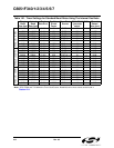


C8051F340/1/2/3/4/5/6/7
222 Rev. 0.5
19.3. Configuration and Operation
UART1 provides standard asynchronous, full duplex communication. It can operate in a point-to-point
serial communications application, or as a node on a multi-processor serial interface. To operate in a
point-to-point application, where there are only two devices on the serial bus, the MCE1 bit in SMOD1
should be cleared to ‘0’. For operation as part of a multi-processor communications bus, the MCE1 and
XBE1 bits should both be set to ‘1’. In both types of applications, data is transmitted from the microcontrol
-
ler on the TX1 pin, and received on the RX1 pin. The TX1 and RX1 pins are configured using the crossbar
and the Port I/O registers, as detailed in
Section “15. Port Input/Output” on page 147.
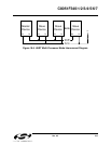
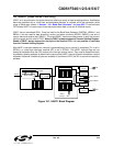
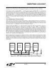
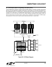
In typical UART communications, The transmit (TX) output of one device is connected to the receive (RX)
input of the other device, either directly or through a bus transceiver, as shown in
Figure 19.5.
Figure 19.5. Typical UART Interconnect Diagram
19.3.1. Data Transmission
Data transmission is double-buffered, and begins when software writes a data byte to the SBUF1 register.
Writing to SBUF1 places data in the Transmit Holding Register, and the Transmit Holding Register Empty
flag (THRE1) will be cleared to ‘0’. If the UARTs shift register is empty (i.e. no transmission is in progress)
the data will be placed in the shift register, and the THRE1 bit will be set to ‘1’. If a transmission is in
progress, the data will remain in the Transmit Holding Register until the current transmission is complete.
The TI1 Transmit Interrupt Flag (SCON1.1) will be set at the end of any transmission (the beginning of the
stop-bit time). If enabled, an interrupt will occur when TI1 is set.
If the extra bit function is enabled (XBE1 = ‘1’) and the parity function is disabled (PE1 = ‘0’), the value of
the TBX1 (SCON1.3) bit will be sent in the extra bit position. When the parity function is enabled (PE1 =
‘1’), hardware will generate the parity bit according to the selected parity type (selected with S1PT[1:0]),
and append it to the data field. Note: when parity is enabled, the extra bit function is not available.
19.3.2. Data Reception
Data reception can begin any time after the REN1 Receive Enable bit (SCON1.4) is set to logic 1. After the
stop bit is received, the data byte will be stored in the receive FIFO if the following conditions are met: the
receive FIFO (3 bytes deep) must not be full, and the stop bit(s) must be logic
1. In the event that the
receive FIFO is full, the incoming byte will be lost, and a Receive FIFO Overrun Error will be generated
(OVR1 in register SCON1 will be set to logic
1). If the stop bit(s) were logic 0, the incoming data will not be
stored in the receive FIFO. If the reception conditions are met, the data is stored in the receive FIFO, and
the RI1 flag will be set. Note: when MCE1 = ‘1’, RI1 will only be set if the extra bit was equal to ‘1’. Data can
be read from the receive FIFO by reading the SBUF1 register. The SBUF1 register represents the oldest
OR
RS-232
C8051Fxxx
RS-232
LEVEL
TRANSLATOR
TX
RX
C8051Fxxx
RX
TX
MCU
RX
TX
PC
COM Port