


C8051F340/1/2/3/4/5/6/7
194 Rev. 0.5
17.1. Supporting Documents
It is assumed the reader is familiar with or has access to the following supporting documents:
1. The I2C-Bus and How to Use It (including specifications), Philips Semiconductor.
2. The I2C-Bus Specification -- Version 2.0, Philips Semiconductor.
3. System Management Bus Specification -- Version 1.1, SBS Implementers Forum.
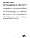
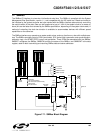
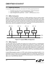
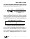
17.2. SMBus Configuration
Figure 17.2 shows a typical SMBus configuration. The SMBus specification allows any recessive voltage
between 3.0 V and 5.0 V; different devices on the bus may operate at different voltage levels. The bi-direc-
tional SCL (serial clock) and SDA (serial data) lines must be connected to a positive power supply voltage
through a pull-up resistor or similar circuit. Every device connected to the bus must have an open-drain or
open-collector output for both the SCL and SDA lines, so that both are pulled high (recessive state) when
the bus is free. The maximum number of devices on the bus is limited only by the requirement that the rise
and fall times on the bus not exceed 300
ns and 1000 ns, respectively.
Figure 17.2. Typical SMBus Configuration
17.3. SMBus Operation
Two types of data transfers are possible: data transfers from a master transmitter to an addressed slave
receiver (WRITE), and data transfers from an addressed slave transmitter to a master receiver (READ).
The master device initiates both types of data transfers and provides the serial clock pulses on SCL. The
SMBus interface may operate as a master or a slave, and multiple master devices on the same bus are
supported. If two or more masters attempt to initiate a data transfer simultaneously, an arbitration scheme
is employed with a single master always winning the arbitration. Note that it is not necessary to specify one
device as the Master in a system; any device who transmits a START and a slave address becomes the
master for the duration of that transfer.
A typical SMBus transaction consists of a START condition followed by an address byte (Bits7-1: 7-bit
slave address; Bit0: R/W direction bit), one or more bytes of data, and a STOP condition. Each byte that is
received (by a master or slave) must be acknowledged (ACK) with a low SDA during a high SCL (see
Figure 17.3). If the receiving device does not ACK, the transmitting device will read a NACK (not acknowl-
edge), which is a high SDA during a high SCL.
VDD = 5V
Master
Device
Slave
Device 1
Slave
Device 2
VDD = 3V VDD = 5V VDD = 3V
SD
A
SCL