


Rev. 0.5 29
C8051F340/1/2/3/4/5/6/7
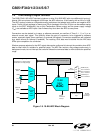
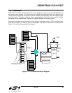
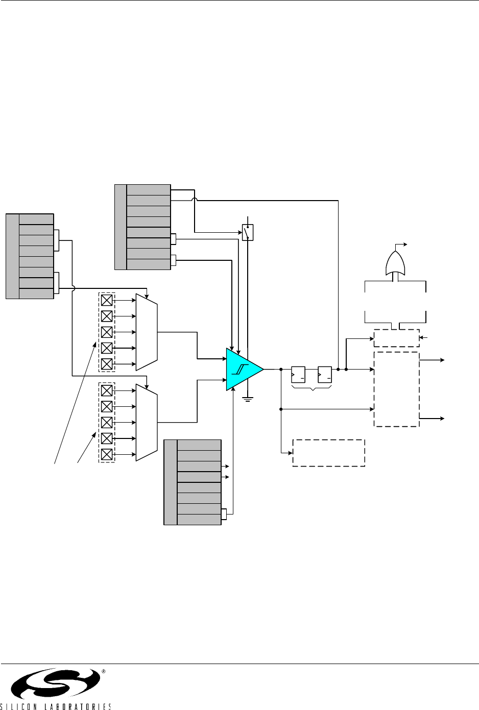
1.10. Comparators
C8051F340/1/2/3/4/5/6/7 devices include two on-chip voltage comparators that are enabled/disabled and
configured via user software. Port I/O pins may be configured as comparator inputs via a selection mux.
Two comparator outputs may be routed to a Port pin if desired: a latched output and/or an unlatched (asyn
-
chronous) output. Comparator response time is programmable, allowing the user to select between
high-speed and low-power modes. Positive and negative hysteresis are also configurable.
Comparator interrupts may be generated on rising, falling, or both edges. When in IDLE mode, these inter-
rupts may be used as a “wake-up” source. Comparator0 may also be configured as a reset source.
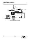
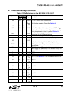
Figure 1.10 shows the Comparator0 block diagram.
Figure 1.10. Comparator0 Block Diagram
VDD
CPTnCN
Reset Decision Tree
(Comprator 0 Only)
+
-
Crossbar
Interrupt
Logic
Q
Q
SET
CLR
D
Q
Q
SET
CLR
D
(SYNCHRONIZER)
GND
CPn +
CPn -
CPnEN
CPnOUT
CPnRIF
CPnFIF
CPnHYP1
CPnHYP0
CPnHYN1
CPnHYN0
CPTnMD
CPnRIE
CPnFIE
CPnMD1
CPnMD0
CPn
CPnA
CPn
Rising-edge
CPn
Falling-edge
CPn
Interrupt
CPnRIE
CPnFIE
CPTnMX
CMXnN1
CMXnN0
CMXnP1
CMXnP0
CMXnN2
CMXnP2
Port I/O connection options vary with
package (32-pin or 48-pin)