


Rev. 0.5 279
C8051F340/1/2/3/4/5/6/7
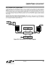
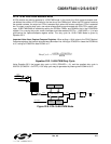
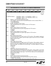
23. C2 Interface
C8051F340/1/2/3/4/5/6/7 devices include an on-chip Silicon Labs 2-Wire (C2) debug interface to allow
Flash programming and in-system debugging with the production part installed in the end application. The
C2 interface uses a clock signal (C2CK) and a bi-directional C2 data signal (C2D) to transfer information
between the device and a host system. See the C2 Interface Specification for details on the C2 protocol.
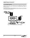
23.1. C2 Interface Registers
The following describes the C2 registers necessary to perform Flash programming functions through the
C2 interface. All C2 registers are accessed through the C2 interface as described in the C2 Interface Spec
-
ification.
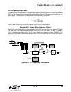
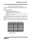
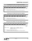
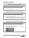
C2 Register Definition 23.1. C2ADD: C2 Address
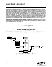
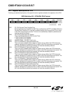
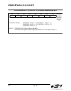
C2 Register Definition 23.2. DEVICEID: C2 Device ID
Bits7–0: The C2ADD register is accessed via the C2 interface to select the target Data register for
C2 Data Read and Data Write commands.
Reset Value
00000000
Bit7 Bit6 Bit5 Bit4 Bit3 Bit2 Bit1 Bit0
Address Description
0x00 Selects the Device ID register for Data Read instructions
0x01 Selects the Revision ID register for Data Read instructions
0x02 Selects the C2 Flash Programming Control register for Data Read/Write instructions
0xAD Selects the C2 Flash Programming Data register for Data Read/Write instructions
This read-only register returns the 8-bit device ID: 0x0F (C8051F340/1/2/3/4/5/6/7).
Reset Value
00001111
Bit7 Bit6 Bit5 Bit4 Bit3 Bit2 Bit1 Bit0