


Rev. 0.5 125
C8051F340/1/2/3/4/5/6/7
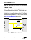
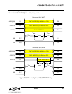
13.6.3. Split Mode with Bank Select
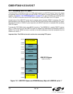
When EMI0CF.[3:2] are set to ‘10’, the XRAM memory map is split into two areas, on-chip space and
off-chip space.
• Effective addresses below the internal XRAM size boundary will access on-chip XRAM space.
• Effective addresses above the internal XRAM size boundary will access off-chip space.
• 8-bit MOVX operations use the contents of EMI0CN to determine whether the memory access is
on-chip or off-chip. The upper 8-bits of the Address Bus A[15:8] are determined by EMI0CN, and the
lower 8-bits of the Address Bus A[7:0] are determined by R0 or R1. All 16-bits of the Address Bus
A[15:0] are driven in “Bank Select” mode.
• 16-bit MOVX operations use the contents of DPTR to determine whether the memory access is
on-chip or off-chip, and the full 16-bits of the Address Bus A[15:0] are driven during the off-chip trans
-
action.
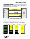
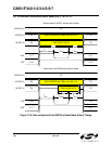
13.6.4. External Only
When EMI0CF[3:2] are set to ‘11’, all MOVX operations are directed to off-chip space. On-chip XRAM is
not visible to the CPU. This mode is useful for accessing off-chip memory located between 0x0000 and the
internal XRAM size boundary.
• 8-bit MOVX operations ignore the contents of EMI0CN. The upper Address bits A[15:8] are not driven
(identical behavior to an off-chip access in “Split Mode without Bank Select” described above). This
allows the user to manipulate the upper address bits at will by setting the Port state directly. The lower
8-bits of the effective address A[7:0] are determined by the contents of R0 or R1.
• 16-bit MOVX operations use the contents of DPTR to determine the effective address A[15:0]. The full
16-bits of the Address Bus A[15:0] are driven during the off-chip transaction.
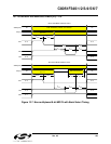
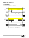
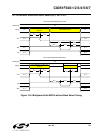
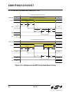
13.7. Timing
The timing parameters of the External Memory Interface can be configured to enable connection to
devices having different setup and hold time requirements. The Address Setup time, Address Hold time, /
RD and /WR strobe widths, and in multiplexed mode, the width of the ALE pulse are all programmable in
units of SYSCLK periods through EMI0TC, shown in
SFR Definition 13.3, and EMI0CF[1:0].
The timing for an off-chip MOVX instruction can be calculated by adding 4 SYSCLK cycles to the timing
parameters defined by the EMI0TC register. Assuming non-multiplexed operation, the minimum execution
time for an off-chip XRAM operation is 5 SYSCLK cycles (1 SYSCLK for /RD or /WR pulse + 4 SYSCLKs).
For multiplexed operations, the Address Latch Enable signal will require a minimum of 2 additional
SYSCLK cycles. Therefore, the minimum execution time for an off-chip XRAM operation in multiplexed
mode is 7 SYSCLK cycles (2 for /ALE + 1 for /RD or /WR + 4). The programmable setup and hold times
default to the maximum delay settings after a reset.
Table 13.1 lists the AC parameters for the External
Memory Interface, and Figure 13.5 through Figure 13.10 show the timing diagrams for the different Exter-
nal Memory Interface modes and MOVX operations.