


Rev. 0.5 109
C8051F340/1/2/3/4/5/6/7
12. Flash Memory
On-chip, re-programmable Flash memory is included for program code and non-volatile data storage. The
Flash memory can be programmed in-system through the C2 interface or by software using the MOVX
instruction. Once cleared to logic 0, a Flash bit must be erased to set it back to logic 1. Flash bytes would
typically be erased (set to 0xFF) before being reprogrammed. The write and erase operations are automat
-
ically timed by hardware for proper execution; data polling to determine the end of the write/erase opera-
tion is not required. Code execution is stalled during a Flash write/erase operation. Refer to Table 12.1 for
complete Flash memory electrical characteristics.
12.1. Programming The Flash Memory
The simplest means of programming the Flash memory is through the C2 interface using programming
tools provided by Silicon Labs or a third party vendor. This is the only means for programming a non-initial
-
ized device. For details on the C2 commands to program Flash memory, see Section “23. C2 Interface”
on page 279.
To ensure the integrity of Flash contents, the V
DD
Monitor must be enabled before writing and/or
erasing Flash memory from software. If a write or erase attempt is made while the V
DD
monitor is
disabled, it will cause a Flash Error device reset.
12.1.1. Flash Lock and Key Functions
Flash writes and erases by user software are protected with a lock and key function. The Flash Lock and
Key Register (FLKEY) must be written with the correct key codes, in sequence, before Flash operations
may be performed. The key codes are: 0xA5, 0xF1. The timing does not matter, but the codes must be
written in order. If the key codes are written out of order, or the wrong codes are written, Flash writes and
erases will be disabled until the next system reset. Flash writes and erases will also be disabled if a Flash
write or erase is attempted before the key codes have been written properly. The Flash lock resets after
each write or erase; the key codes must be written again before a following Flash operation can be per
-
formed. The FLKEY register is detailed in SFR Definition 12.2.
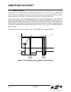
12.1.2. Flash Erase Procedure
The Flash memory can be programmed by software using the MOVX write instruction with the address and
data byte to be programmed provided as normal operands. Before writing to Flash memory using MOVX,
Flash write operations must be enabled by: (1) Writing the Flash key codes in sequence to the Flash Lock
register (FLKEY); and (2) Setting the PSWE Program Store Write Enable bit (PSCTL.0) to logic 1 (this
directs the MOVX writes to target Flash memory). The PSWE bit remains set until cleared by software.
A write to Flash memory can clear bits to logic 0 but cannot set them; only an erase operation can set bits
to logic 1 in Flash.
A byte location to be programmed must be erased before a new value is written.
The Flash memory is organized in 512-byte pages. The erase operation applies to an entire page (setting
all bytes in the page to 0xFF). To erase an entire 512-byte page, perform the following steps:
Step 1. Disable interrupts (recommended).
Step 2. Write the first key code to FLKEY: 0xA5.
Step 3. Write the second key code to FLKEY: 0xF1.
Step 4. Set the PSEE bit (register PSCTL).
Step 5. Set the PSWE bit (register PSCTL).
Step 6. Using the MOVX instruction, write a data byte to any location within the 512-byte page to
be erased.
Step 7. Clear the PSWE bit (register PSCTL).
Step 8. Clear the PSEE bit (register PSCTI).